Electric in-situ buckle background method for graphene plasmon reinforcing infrared spectroscopy detection

A plasmon enhancement, infrared spectroscopy technology, applied in color/spectral property measurement, nanotechnology, etc., can solve the problems of limited detection capability, improved repeatability, and narrow enhancement band.

Active Publication Date: 2016-03-16
THE NAT CENT FOR NANOSCI & TECH NCNST OF CHINA
View PDF6 Cites 11 Cited by
  • Summary
  • Abstract
  • Description
  • Claims
  • Application Information

AI Technical Summary

Problems solved by technology

However, at present, this technology has the defects of very narrow enhanced band, greatly limited detection ca

Method used


Image

  • Electric in-situ buckle background method for graphene plasmon reinforcing infrared spectroscopy detection
  • Electric in-situ buckle background method for graphene plasmon reinforcing infrared spectroscopy detection
  • Electric in-situ buckle background method for graphene plasmon reinforcing infrared spectroscopy detection

Examples


Embodiment 1

[0049] In this example, CaF 2 As an example of a dielectric layer, the graphene plasmonic device of the present invention is used to perform infrared detection on a polyethylene oxide (PEO) film.

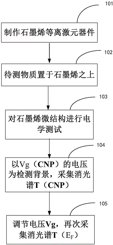
[0050] 1. Conduct electrical tests on the graphene microstructure, measure the transport curve of graphene, and obtain the voltage corresponding to the Dirac point of graphene.

[0051] Measure the Ids-Vg transport curve of graphene, and read the voltage Vg(CNP) corresponding to the Dirac point of graphene. According to this example, with CaF 2 The Ids-Vg transport curve of graphene measured as a dielectric layer, as shown in Figure 5(a), shows a bipolar "V" shape. The gate voltage at 5 V corresponds to the neutral position of graphene charge doping (ie the graphene Dirac point).

[0052] 2. Infrared signal detection is carried out by using the method of subtracting the background in situ.

[0053] a) With the voltage of Vg(CNP) (i.e. 5V) as the detection background, select a ce...

Embodiment 2

[0057] In this example, CaF 2 As an example of a dielectric layer, the graphene plasmonic device of the present invention is used for infrared detection of a single layer of boron nitride (BN).

[0058] 1. Conduct electrical tests on the graphene microstructure, measure the transport curve of graphene, and obtain the voltage corresponding to the Dirac point of graphene.

[0059] Measure the Ids-Vg transport curve of graphene, and read the voltage Vg(CNP) corresponding to the Dirac point of graphene. According to this example, with CaF 2 The Ids-Vg transport curve of graphene measured as a dielectric layer, as shown in Figure 6(a), shows a bipolar "V" shape. The gate voltage at 5 V corresponds to the neutral position of graphene charge doping (ie the graphene Dirac point).

[0060] 2. Infrared signal detection is carried out by using the method of subtracting the background in situ.

[0061] a) With the voltage of Vg(CNP) (i.e. 5V) as the detection background, select a cert...


PUM

PropertyMeasurementUnit
Apertureaaaaaaaaaa

Abstract

The invention provides an electric in-situ buckle background method for graphene plasmon reinforcing infrared spectroscopy detection. The method comprises the following steps: 1) preparing an infrared reinforcing and detecting device for a graphene plasmon component; 2) putting a to-be-detected object onto a graphene micro-structure; 3) performing an electrical test on the graphene micro-structure: measuring an Ids-Vg transport curve of graphene and reading a voltage Vg(CNP) corresponding to a Dirac point of the graphene; 4) performing infrared signal detection by utilizing the in-situ buckle background method, comprising the following sub-steps: a) by taking the voltage Vg(CNP) as the detecting background, collecting an extinction spectrum T (CNP); and b) adjusting the voltage Vg, reinforcing sample signals at various degrees by utilizing positive and negative voltages above or below the Dirac point, collecting the extinction spectrum T (EF) again, and confirming the step length of the voltage Vg according to the natures and specific measured scopes of different dielectric layer materials.

Description

technical field [0001] The invention relates to the technical field of infrared light detection, in particular to a graphene plasmonic element device for enhancing infrared spectrum detection and an electrical in-situ deduction background method for enhancing infrared spectrum detection. Background technique [0002] Infrared radiation contains rich objective information, and its detection has attracted much attention. Infrared detectors have covered short-wave, medium-wave and long-wave ranges, and have been widely used in military and civilian fields. Its detection principle is to use the photoelectric conversion performance of the material to convert the photon signal of infrared radiation into an electronic signal, and combine it with an external circuit to achieve the goal of detecting infrared light signals. [0003] Graphene is a two-dimensional crystal composed of a single layer of carbon atoms, and the thickness of a single layer of graphite is about 0.35nm. Curre...

Claims


Application Information

Patent Timeline
IPC IPC(8): G01N21/35B82Y40/00
CPCB82Y40/00G01N21/35
Inventor 胡海胡德波白冰刘瑞娜杨晓霞戴庆
Owner THE NAT CENT FOR NANOSCI & TECH NCNST OF CHINA
Why Eureka
Try Eureka