
Method for grinding and polishing CdZnTe wafer without wax

A cadmium zinc telluride wafer, grinding and polishing technology, applied in the field of wax-free grinding and polishing of cadmium zinc telluride wafers, can solve the problems of increased fragmentation rate, time-consuming chip removal process, difficult to remove, etc., to achieve accurate wafer thickness control, reduce cracks and Scratch, improve the effect of grinding and polishing quality

Inactive Publication Date: 2016-03-23
SHANGHAI INST OF TECHNICAL PHYSICS - CHINESE ACAD OF SCI
View PDF4 Cites 5 Cited by
  • Summary
  • Abstract
  • Description
  • Claims
  • Application Information

AI Technical Summary

Problems solved by technology

The traditional method has the following disadvantages: (1) The thickness of the paste wax layer is uneven, and the flatness of the processed material is not good
(2) The process of heating the sticky film and melting the wax to take the film is time-consuming and reduces the process efficiency
(3) Grinding and polishing debris is easy to adhere to the wafer, so it is easy to collide or scratch the wafer surface, reducing the quality of the wafer surface
(4) Even after repeated cleaning with multiple organic reagents, wax sometimes remains and is difficult to remove. Contamination of materials will affect the quality of subsequent processes
However, the above method must be drilled or made a slot according to the standard size of the wafer to fix the position of the wafer, so it can only be used for wafers with standard sizes, and is not suitable for processing wafers with irregular shapes and thicknesses.
In addition, due to the fixed limit around the wafer, during the grinding and polishing process, the wafer will rigidly collide with the surrounding slots. Since the CdZnTe crystal is a soft and brittle material, it is easy to break and cleave. Large-sized wafer processing, using this kind of wax-free polishing method will significantly increase the debris rate

Method used


Image

  • Method for grinding and polishing CdZnTe wafer without wax
  • Method for grinding and polishing CdZnTe wafer without wax

Examples


Embodiment 1

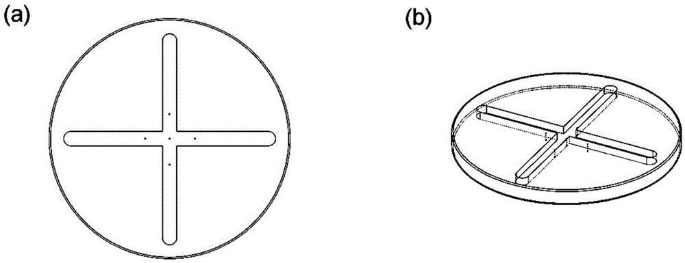
[0022] 1 Upper wafer: first place the groove of the transfer plate with the small hole facing down on the vacuum adsorption surface of the grinding and polishing fixture, and then place the rectangular wafer with a size of 3cmX4cm horizontally on the turntable with the surface to be polished facing upward. On the transfer tray, gently move the wafer to the center of the transfer tray, so that the wafer covers all the small holes on the transfer tray. Connect the grinding and polishing fixture with the vacuum generator, the vacuum is converted by the adapter plate, and the groove and the small hole will generate vacuum immediately, and the wafer will be adsorbed and fixed.

[0023] 23um alumina grinding: Prepare alumina particle suspension grinding liquid with a volume ratio of 3um alumina powder to deionized water of 1:10, stir evenly and set aside. Use a flat glass grinding disc, set the rotation speed of the grinding disc to 5rpm / min, and the drop rate of the grinding liquid...

Embodiment 2

[0029] 1 Upper wafer: first place the groove of the transfer plate with the small hole facing downward on the vacuum adsorption surface of the grinding and polishing fixture, and then place the square wafer with a size of 4cmX4cm horizontally on the turntable with the surface to be polished facing upward. On the transfer tray, gently move the wafer to the center of the transfer tray, so that the wafer covers all the small holes on the transfer tray. Connect the grinding and polishing fixture with the vacuum generator, the vacuum is converted by the adapter plate, and the groove and the small hole will generate vacuum immediately, and the wafer will be adsorbed and fixed.

[0030]23um alumina grinding: Prepare alumina particle suspension grinding liquid with a volume ratio of 3um alumina powder to deionized water of 1:10, stir evenly and set aside. Use a flat glass grinding disc, set the rotating speed of the grinding disc to 20rpm / min, and the drop rate of the grinding liquid ...

Embodiment 3

[0036] 1. Upper wafer: firstly place the groove of the transfer plate with the small hole facing downward on the vacuum adsorption surface of the grinding and polishing fixture, and then place the irregularly shaped wafer with a size of more than 2cmX2cm horizontally with the grinding and polishing surface facing upward On the transfer plate, gently move the wafer to the center of the transfer plate so that the wafer covers all the small holes on the transfer plate. Connect the grinding and polishing fixture with the vacuum generator, the vacuum is converted by the adapter plate, and the groove and the small hole will generate vacuum immediately, and the wafer will be adsorbed and fixed.

[0037] 23um alumina grinding: Prepare alumina particle suspension grinding liquid with a volume ratio of 3um alumina powder to deionized water of 1:10, stir evenly and set aside. Use a flat glass grinding disc, set the rotation speed of the grinding disc to 30rpm / min, and the drop rate of th...


PUM


Abstract

The invention discloses a method for grinding and polishing a CdZnTe wafer without wax. The method includes the steps that firstly, a grinding and polishing clamp joint plate is designed and manufactured and horizontally placed on an adsorption plane of a grinding and polishing clamp; the wafer is placed in the center of the joint plate to cover all small vacuum flow guide holes in the joint plate; a grinding clamp is connected with a vacuum generator, and the wafer is adsorbed and fixed; and the wafer is ground through a 3-micron aluminum oxide water solution, 30-50 microns of the wafer is removed, and then a Chemlox polishing liquid chemical machine produced by the Logitech enterprise in England is used for polishing for 2-5 min, and the high-flatness CdZnTe wafer is obtained after cleaning. The method has the beneficial effects that a heating wafer sticking and wax melting wafer taking are not needed, the thickness of the wafer is controlled more accurately, and flatness is higher; the method is suitable for wafers of different sizes, shapes and thicknesses, and practicability is high; cleaning is easy after grinding and polishing, and secondary contamination cannot be caused on the wafer; and cracks and scratches can be reduced, and the grinding and polishing quality is improved.

Description

technical field [0001] The invention relates to a semiconductor material grinding and polishing processing technology, in particular to a method for wax-free grinding and polishing of CdZnTe wafers. The invention is suitable for grinding and polishing equipment whose sample holder is a vacuum adsorption type, and is suitable for wafers with a size of more than 2cmX2cm and a thickness of 100um-5000um. Background technique [0002] Cadmium Zinc Telluride (CdZnTe, CZT) material can be matched perfectly with the lattice constant of HgCdTe by adjusting the zinc composition range, so it is the preferred substrate for HgCdTe infrared focal plane detectors. In addition, CdZnTe can also be used to prepare X and γ-ray detectors, and has a wide range of applications in aerospace remote sensing technology, security inspection technology, medical diagnostic technology, and weaponry. However, in addition to the crystal defects generated during the material growth process, quality defects...

Claims


Application Information

Patent Timeline
Patent Type & Authority Applications(China)
IPC IPC(8): B24B1/00
CPCB24B1/00
Inventor 虞慧娴陆丞周梅华孙士文
Owner SHANGHAI INST OF TECHNICAL PHYSICS - CHINESE ACAD OF SCI
Learn More