Delta channel doping SiC vertical power MOS device manufacturing method
What is Al technical title?
Al technical title is built by PatSnap Al team. It summarizes the technical point description of the patent document.
A technology of MOS device and manufacturing method, applied in the field of microelectronics
Active Publication Date: 2016-04-06
XIDIAN NINGBO INFORMATION TECH INST
View PDF4 Cites 7 Cited by
Summary
Abstract
Description
Claims
Application Information
AI Technical Summary
This helps you quickly interpret patents by identifying the three key elements:
Problems solved by technology
Method used
Benefits of technology
Problems solved by technology
Although many research groups at home and abroad hope to improve the conduction characteristics of the device by improving the device structure and surface structure, such as forming multi-sub-accumulation regions on the device surface, and UMOS structures, etc., due to the formation of multi-sub-regions on the surface, Many devices are normally open
Method used
Image
Click on the blue label to locate the original text in one second.
Reading with bidirectional positioning of images and text.
Examples
Embodiment 1
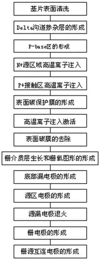
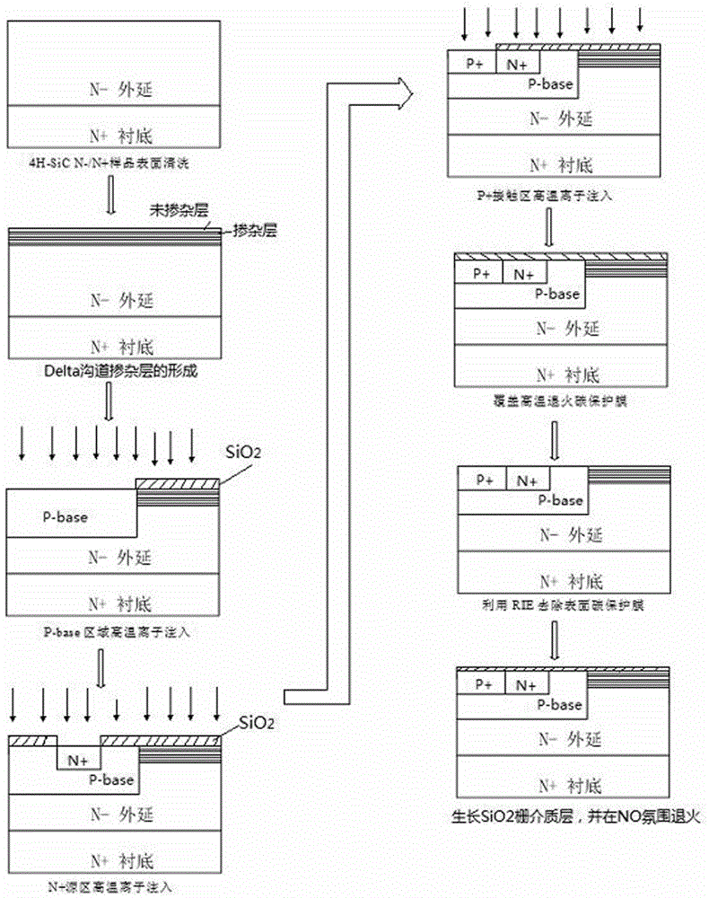
[0095] refer to figure 1 , image 3 and Figure 4 , the preparation and implementation steps of the first embodiment of the present invention are as follows:
[0096] Step 1. Use the standard cleaning method RCA to clean the surface of the 4H-SiCN- / N+ type SiC epitaxial wafer. The specific cleaning process is as follows:
[0097] (1a) Soak the 4H-SiCN- / N+ type SiC epitaxial wafer in acetone and absolute ethanol for 5 minutes each, and then rinse with deionized water to remove the grease on the surface of the SiC epitaxial wafer;
[0098] (1b) Place the SiC epitaxial wafer after the first cleaning in H 2 SO 4 :H 2 o 2 =1:1 (volume ratio) solution soaked for 15min, H 2 SO 4 The concentration is 98%, H 2 o 2 The concentration is 27%, then rinse with deionized water;
[0099] (1c) Place the SiC epitaxial wafer after the second cleaning in HF:H 2 Soak in the solution of O=1:10 (volume ratio) for 1min to rinse off the natural oxide layer, the concentration of HF acid is ...
Embodiment 2
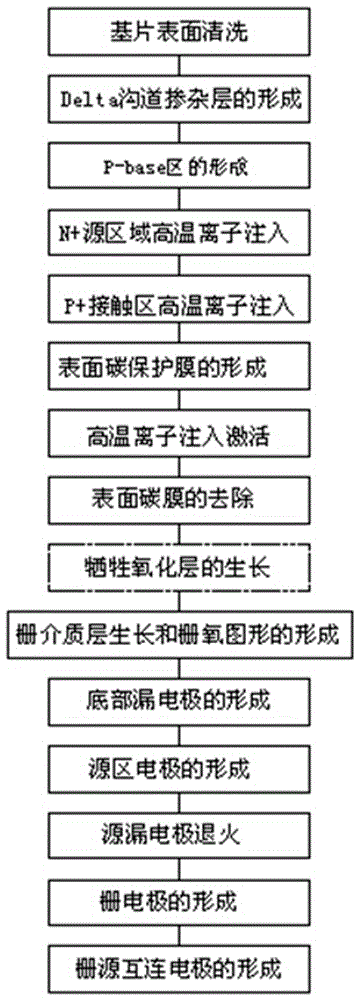
[0228] Compared with Example 1, this example is based on Example 1, after removing the carbon protective film on the front of the N- / N+ SiC epitaxy and growing SiO over a large area 2A growth process of a sacrificial oxide layer is added between the gate dielectric layers, which can more effectively reduce the interface damage caused by high-temperature ion implantation annealing, and effectively improve the flatness of the interface.
[0229] Such as figure 2 , Figure 5 and Image 6 As shown, the implementation steps of this embodiment 2 are as follows (other process contents not mentioned are the same as the previous embodiment):
[0230] Step I, growth of sacrificial oxide layer:
[0231] (Ia) Put the SiC epitaxial wafer that has undergone high-temperature annealing into a high-temperature oxidation furnace, oxidize the surface of the SiC epitaxial wafer under pure dry oxygen at 1200 ° C for 30 minutes, and generate SiO with a thickness of 20 nm on the front side of th...
PUM
Property
Measurement
Unit
thickness
aaaaa
aaaaa
thickness
aaaaa
aaaaa
thickness
aaaaa
aaaaa
Abstract
The invention provides a Delta channel doping SiC vertical power MOS device manufacturing method. The method comprises the steps of: cleaning the surface of an N-/N+ type SiC epitaxial wafer; carrying out layered doping in a CVD furnace; etching out a P-base region and injecting high temperature Al irons; etching out an N+ doping source region and injecting high temperature N irons; etching out a P+ contact region and injecting high temperature Al irons; forming a carbon protection film on the surface of the N-/N+ type SiC epitaxial wafer; annealing high temperature iron injection; removing the surface carbon film; carrying out acid cleaning; growing a SiO2 insulating layer; growing a bottom drain electrode; smearing stripping glue and a photoresist, etching out a source contact hole, carrying out source metal deposition, and stripping the source metal to form a source pattern; annealing source and drain electrodes; forming a grid electrode; and forming a grid and source interconnection electrode. According to the invention, the channel effective migration rate of the vertical power MOS device is effectively improved, the threshold voltage of the device is reduced, and the conduction characteristic of the vertical power device is improved.
Description
technical field [0001] The invention relates to the technical field of microelectronics, in particular to a method for manufacturing a Delta channel doped SiC vertical power MOS device. To reduce the threshold voltage of the SiC vertical power MOS device, increase the effective mobility of the channel, thereby improving the conduction characteristics of the power MOS device. Background technique [0002] SiC has unique physical, chemical and electrical properties, and is a semiconductor material with great development potential in extreme applications such as high temperature, high frequency, high power and radiation resistance. The improvement of the conduction characteristics and transient characteristics of SiC power MOSFETs has always been a difficulty in power devices. Although many research groups at home and abroad hope to improve the conduction characteristics of the device by improving the device structure and surface structure, such as forming multi-sub-accumulati...
Claims
Application Information
Patent Timeline
Application Date:The date an application was filed.
Publication Date:The date a patent or application was officially published.
First Publication Date:The earliest publication date of a patent with the same application number.
Issue Date:Publication date of the patent grant document.
PCT Entry Date:The Entry date of PCT National Phase.
Estimated Expiry Date:The statutory expiry date of a patent right according to the Patent Law, and it is the longest term of protection that the patent right can achieve without the termination of the patent right due to other reasons(Term extension factor has been taken into account ).
Invalid Date:Actual expiry date is based on effective date or publication date of legal transaction data of invalid patent.