SOI base-based low-leakage and low-capacitance TVS array and preparation method thereof

A low-leakage, low-capacitance technology, which is applied in circuits, electrical components, and electric solid-state devices, can solve problems such as tunnel breakdown, thermal effects, and large leakage currents, so as to suppress the interference of pulse currents, avoid data transmission errors, and produce The effect of simple method

Active Publication Date: 2016-04-13
SHANGHAI CHANGYUAN WAYON MICROELECTRONICS
View PDF6 Cites 11 Cited by
  • Summary
  • Abstract
  • Description
  • Claims
  • Application Information

AI Technical Summary

Problems solved by technology

[0008] Another disadvantage of TVS prepared by the traditional process is the large leakage current. Usually TVS diodes work in a reverse bias state. When the reverse voltage at both ends of the TVS is lower than the avalanche breakdown voltage of the PN junction diode material, tunneling often occurs. Piercing effect, causing tunnel breakdown, making the reverse

Method used


Image

  • SOI base-based low-leakage and low-capacitance TVS array and preparation method thereof
  • SOI base-based low-leakage and low-capacitance TVS array and preparation method thereof
  • SOI base-based low-leakage and low-capacitance TVS array and preparation method thereof

Examples


Embodiment Construction

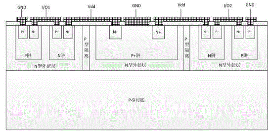
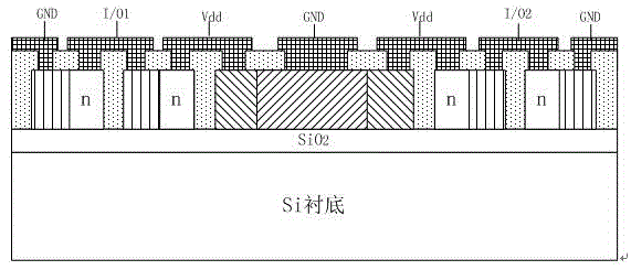
[0050] Such as figure 2 As shown in the structural diagram of the low-leakage and low-capacitance TVS device using the SOI substrate in the present invention, a low-leakage and low-capacitance TVS array based on the SOI substrate, with the SOI substrate as the main body, includes: n-type SOI substrate, p + region, n+ region, p region, silicon nitride isolation and electrode, the n-type SOI substrate is made of Si substrate, SiO 2 Layer and N-type and / or P-type Si three-layer structure, on the P-type and / or N-type Si substrate by diffusion or ion implantation to form a highly doped PN junction, forming the PN junction region and the central TVS region.

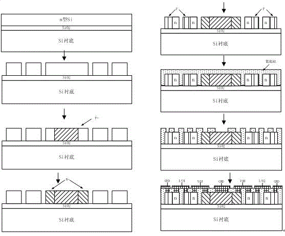
[0051] In order to realize the device of the present invention, in combination with figure 2 with image 3 Given the following implementation steps, such as image 3 as shown,

[0052] step one:

[0053] Take an n-type SOI substrate, clean it to remove surface pollutants, and grow an oxide layer on the surface of the n-t...


PUM


Abstract

The invention relates to an SOI base-based low-leakage and low-capacitance TVS array and a preparation method thereof. The SOI base-based low-leakage and low-capacitance TVS array comprises an n-type SOI base, a p+ region, an n+ region, a p region, a silicon nitride isolator and an electrode, wherein the n-type SOI base is formed by a three-layer structure of an Si substrate, an SiO<2> layer and an n-type Si layer; and highly doped PN junctions are formed on P-type and/N-type SI substrates through diffusion or ion implantation to form a PN junction region and a central TVS region. Compared with a TVS device in the prior art, according to the SOI base-based low-leakage and low-capacitance TVS array, the stray capacitance and the leakage current of the device are effectively reduced; the power consumption of the device is reduced; and the performance of the device is further improved.

Description

technical field [0001] The invention relates to a semiconductor device, in particular to a low-leakage and low-capacity TVS device of an SOI substrate and a preparation method thereof. Background technique [0002] Silicon on Insulator (Silicon on Insulator, SOI) material has a unique material structure different from bulk silicon, thus overcoming many shortcomings of bulk silicon materials, such as eliminating latch-up effects, reducing parasitic capacitance, reducing leakage current, and weakening short channels. effect etc. Therefore, semiconductor devices made of SOI as a substrate material can be widely used in aerospace fields with high speed, low power consumption, high temperature and high reliability requirements. The current mainstream SOI material preparation technologies mainly include: oxygen injection isolation technology (SIMOX), bonding and backside etching (BESOI) technology, smart-cut technology (Smart-Cut) technology, NanoCleave technology and porous sili...

Claims


Application Information

Patent Timeline
IPC IPC(8): H01L27/12H01L29/861H01L21/84
CPCH01L21/84H01L27/1207H01L29/8613
Inventor 霍田佳苏海伟王允张晨旭
Owner SHANGHAI CHANGYUAN WAYON MICROELECTRONICS
Why Eureka
Try Eureka