

Preparation method for efficient solar cell
A solar cell, high-efficiency technology, applied in the field of solar cells, can solve the problem of high cost, achieve the effect of reducing cost consumption, saving cost consumption, and reducing process complexity
- Summary
- Abstract
- Description
- Claims
- Application Information
AI Technical Summary
Problems solved by technology
Method used
Image


Examples
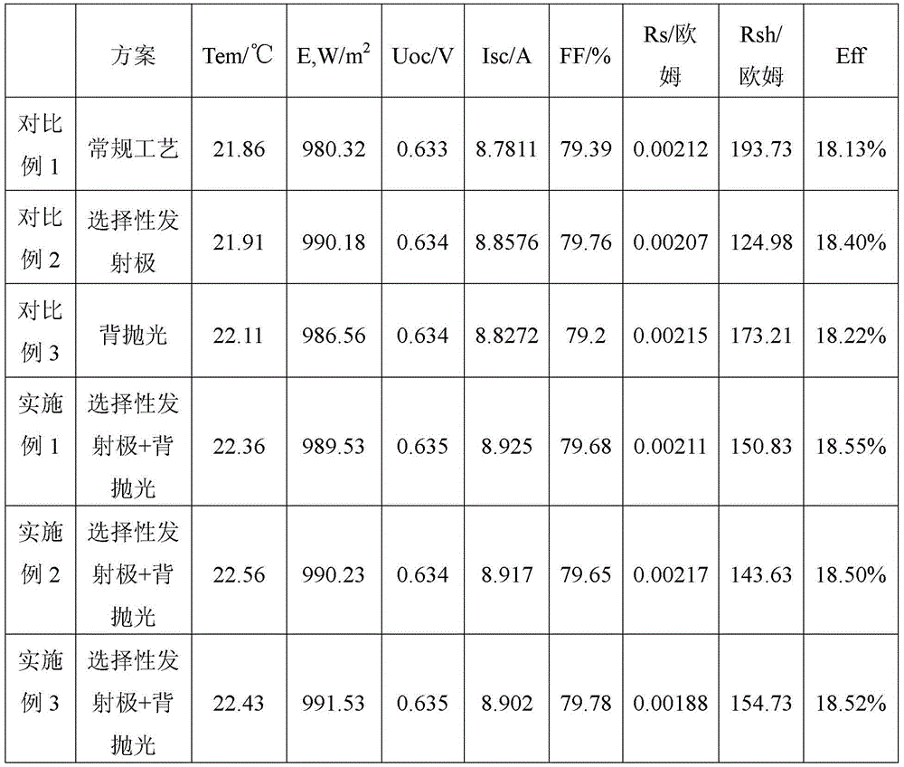
Embodiment 1
[0033] After the raw silicon wafer is cleaned and textured, it is diffused with low square resistance on one side in the atmosphere of phosphorus oxychloride, and the square resistance after diffusion is controlled at 50Ω / ◇; the diffusion side of the silicon wafer is put into the alkali tank chain back polishing machine At the feeding end, the speed of 1.5m / min passes through the alkali tank equipped with 60°C and 20% KOH aqueous solution by mass percentage, and the backside is polished in the KOH aqueous solution for 8.0min. After the backside polishing is completed, the silicon wafer is equipped with pure Wash the residual alkali in the pure water tank of water, dry the upper and lower surfaces of the silicon wafer through the drying section, and take out the silicon wafer from the feeding end smoothly.
[0034] Make a selective emitter:
[0035] a. Put the back-polished silicon wafer into the INK printing machine to print ink on the electrode grid area of the silicon wafe...
Embodiment 2
[0043] After the raw silicon wafer is cleaned and textured, it is diffused in a phosphorus oxychloride atmosphere with low square resistance on one side, and the square resistance after diffusion is controlled at 55Ω / ◇; the diffusion side of the silicon wafer is put into the alkali tank chain back polishing machine At the feeding end, at a rate of 2.2m / min, the backside polishing is carried out in the KOH solution for 5.5min through an alkali tank filled with 80°C and 10% KOH solution by mass percentage concentration. After the backside polishing is completed, the silicon wafer is filled with pure water Wash the residual alkali in the pure water tank, dry the upper and lower surfaces of the silicon wafer through the drying section, and take out the silicon wafer from the feeding end smoothly.
[0044] Make a selective emitter:
[0045] a. Put the back-polished silicon wafer into the INK printing machine to print ink on the electrode grid area of the silicon wafer as a mask, ...
Embodiment 3
[0054] After the raw silicon wafer is cleaned and textured, it is diffused with low square resistance on one side in the atmosphere of phosphorus oxychloride, and the square resistance after diffusion is controlled at 52Ω / ◇; the diffusion side of the silicon wafer is put into the alkali tank chain back polishing machine At the feeding end, at a speed of 1.8m / min, the backside polishing in NaOH aqueous solution was carried out for 6.67min through an alkali tank equipped with 70°C and 35% NaOH aqueous solution by mass percent concentration. Wash the residual alkali in the pure water tank, dry the upper and lower surfaces of the silicon wafer through the drying section, and take out the silicon wafer from the feeding end smoothly.
[0055] Make a selective emitter:
[0056] a. Put the back-polished silicon wafer into the INK printing machine to print ink on the electrode grid area of the silicon wafer as a mask, and dry it.
[0057] b. Put the diffusion surface of the silicon ...
PUM
 Abstract
Description
Claims
Application Information