852nm ultra-narrow line width external-cavity semiconductor laser

An ultra-narrow linewidth, laser technology, applied in the field of 852nm ultra-narrow linewidth external cavity semiconductor lasers, can solve problems such as unfavorable laser frequency stabilization, grating vibration sensitivity, affecting frequency stability and linewidth of external cavity lasers, etc.

Inactive Publication Date: 2016-04-27
BEIJING UNIV OF TECH
View PDF7 Cites 15 Cited by
  • Summary
  • Abstract
  • Description
  • Claims
  • Application Information

AI Technical Summary

Problems solved by technology

In a grating-type external cavity laser, the grating acts as a mode selector and a mirror at the same time. Although its structure is simple, it is difficult to align the external cavity, and the grating is very sensitive to vibration, which is not conducive to the frequency stabilization of the laser.
However, for external cavity lasers based on Fabry-Perot interference filters, the mode selector and mirror are separate components, and the sensitivity of the external cavity to vibr

Method used


Image

  • 852nm ultra-narrow line width external-cavity semiconductor laser
  • 852nm ultra-narrow line width external-cavity semiconductor laser
  • 852nm ultra-narrow line width external-cavity semiconductor laser

Examples


Embodiment Construction

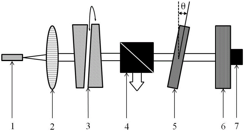
[0019] Such as figure 2 As shown, an 852nm ultra-narrow linewidth external cavity semiconductor laser mainly includes a semiconductor laser gain chip 1 and a collimator lens 2 sequentially placed on the light emitting direction of the semiconductor laser gain chip 1, a rotatable wedge prism pair 3, and a cubic split Beamer 4, rotatable all-dielectric film Fabry-Perot filter 5, total reflection mirror 6 and piezoelectric actuator 7;

[0020] Combine below figure 2 Introduce the method of realizing 852nm ultra-narrow linewidth external cavity semiconductor laser;

[0021] Step 1. Use Metal Organic Chemical Vapor Deposition (MOCVD) epitaxy to grow the epitaxial structure of the semiconductor gain chip, and combine photolithography, etching, oxidation, sputtering, coating and other processes to prepare the gain die. The gain die is at room temperature The lasing wavelength is 852nm, and the light-emitting surface is coated with Al with a reflectivity of less than 0.01%. 2 o ...


PUM

PropertyMeasurementUnit
Full width at half heightaaaaaaaaaa

Abstract

The invention provides an 852nm ultra-narrow line width external-cavity semiconductor laser, which comprises an 852nm laser gain chip, a collimating lens, a rotatable wedge prism pair, a cube beam splitter, a rotatable all-dielectric thin-film fabry-perot light filter, a totally reflecting mirror and a piezoelectric actuator, wherein the collimating lens, the rotatable wedge prism pair, the cube beam splitter, the rotatable all-dielectric thin-film fabry-perot light filter, the totally reflecting mirror and the piezoelectric actuator are sequentially arranged in a light exiting direction of the gain chip; the collimating lens collimates a laser beam and then reflects the laser beam into an external cavity body; the wedge prism pair rotates around an optical axis, so that an incident beam which positively enters the vertical surface of a prism lens deflects; the cube beam splitter outputs one part of light and the other part of light is left in the cavity for oscillation; the fabry-perot light filter can rotate to achieve the target of mode selection for the external cavity; and the totally reflecting mirror can move along the normal direction by combination of the totally reflecting mirror and a PZT. The external-cavity laser can greatly reduce the influence on the frequency caused by mechanical vibration; the mode-hop phenomenon of the laser is avoided; and meanwhile, ultra-narrow line width and linear continuous and adjustable wavelength can be achieved.

Description

technical field [0001] The invention belongs to the technical field of semiconductor lasers, in particular to an 852nm ultra-narrow linewidth external cavity semiconductor laser. Background technique [0002] Ultra-narrow linewidth external cavity semiconductor lasers are widely used in technical fields such as atomic physics, spectroscopy, quantum information, coherent communication, remote sensing and precision measurement, among which 852nm ultra-narrow linewidth external cavity semiconductor lasers are mainly used in ultra-high precision Atomic clocks, short-range communications and other fields. Currently, there are two most common external cavity structures: grating external cavity and Fabry-Perot interference filter external cavity. In the grating-type external cavity laser, the grating acts as a mode selector and a mirror at the same time. Although its structure is simple, it is difficult to align the external cavity, and the grating is very sensitive to vibration, ...

Claims


Application Information

Patent Timeline
IPC IPC(8): H01S5/14
CPCH01S5/141
Inventor 关宝璐潘冠中刘储徐晨李鹏涛刘振杨杨嘉炜
Owner BEIJING UNIV OF TECH
Why Eureka
Try Eureka