

A light-emitting device, its manufacturing method, and display device
A light-emitting device, quantum dot light-emitting technology, applied in chemical instruments and methods, semiconductor/solid-state device manufacturing, light-emitting materials, etc., can solve problems such as increased energy consumption of devices, weakened light emission, and energy loss
- Summary
- Abstract
- Description
- Claims
- Application Information
AI Technical Summary
Problems solved by technology
Method used
Image

Examples
preparation example Construction
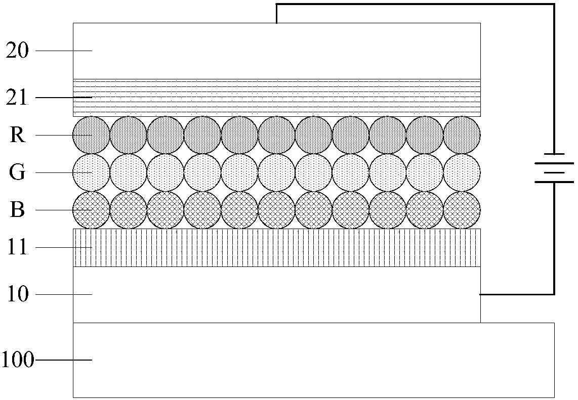
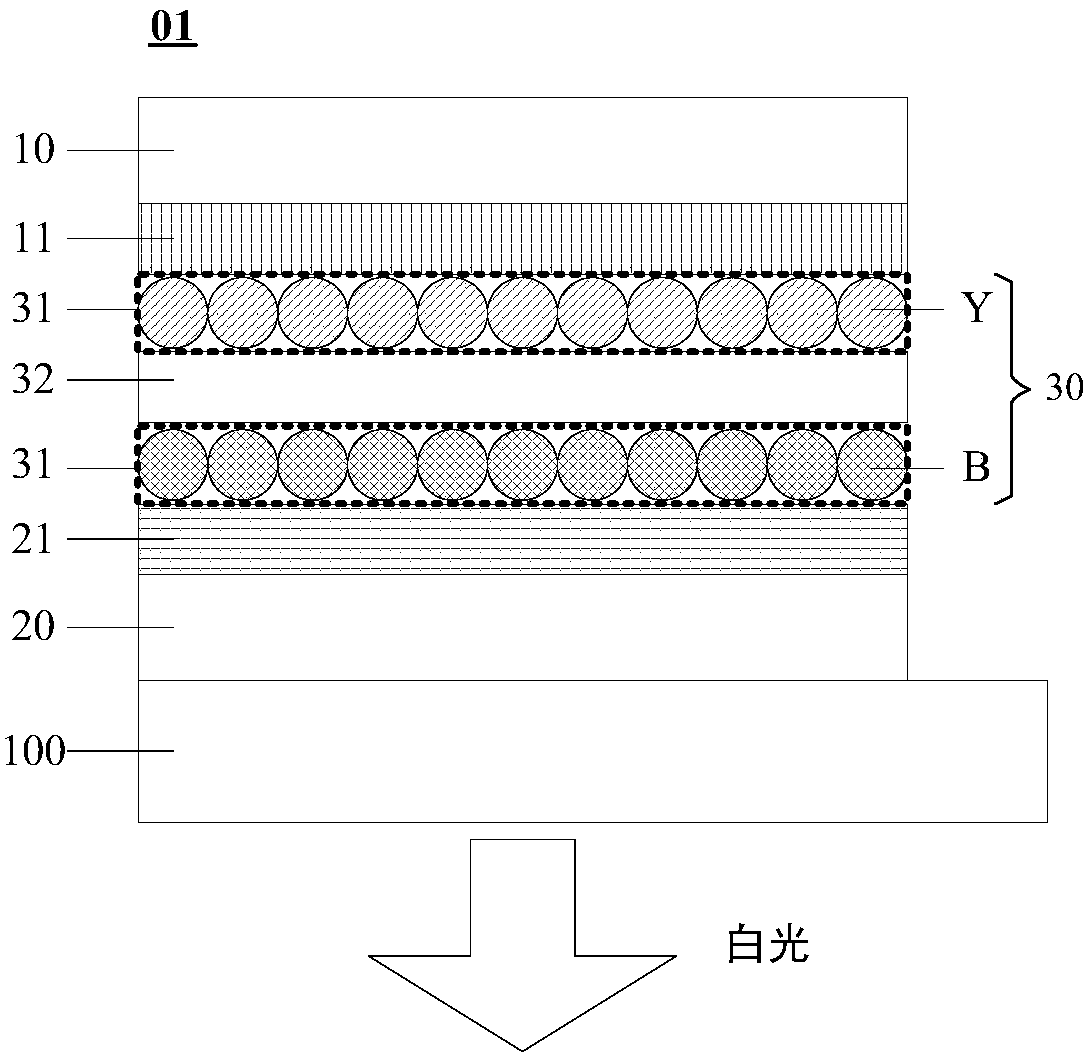
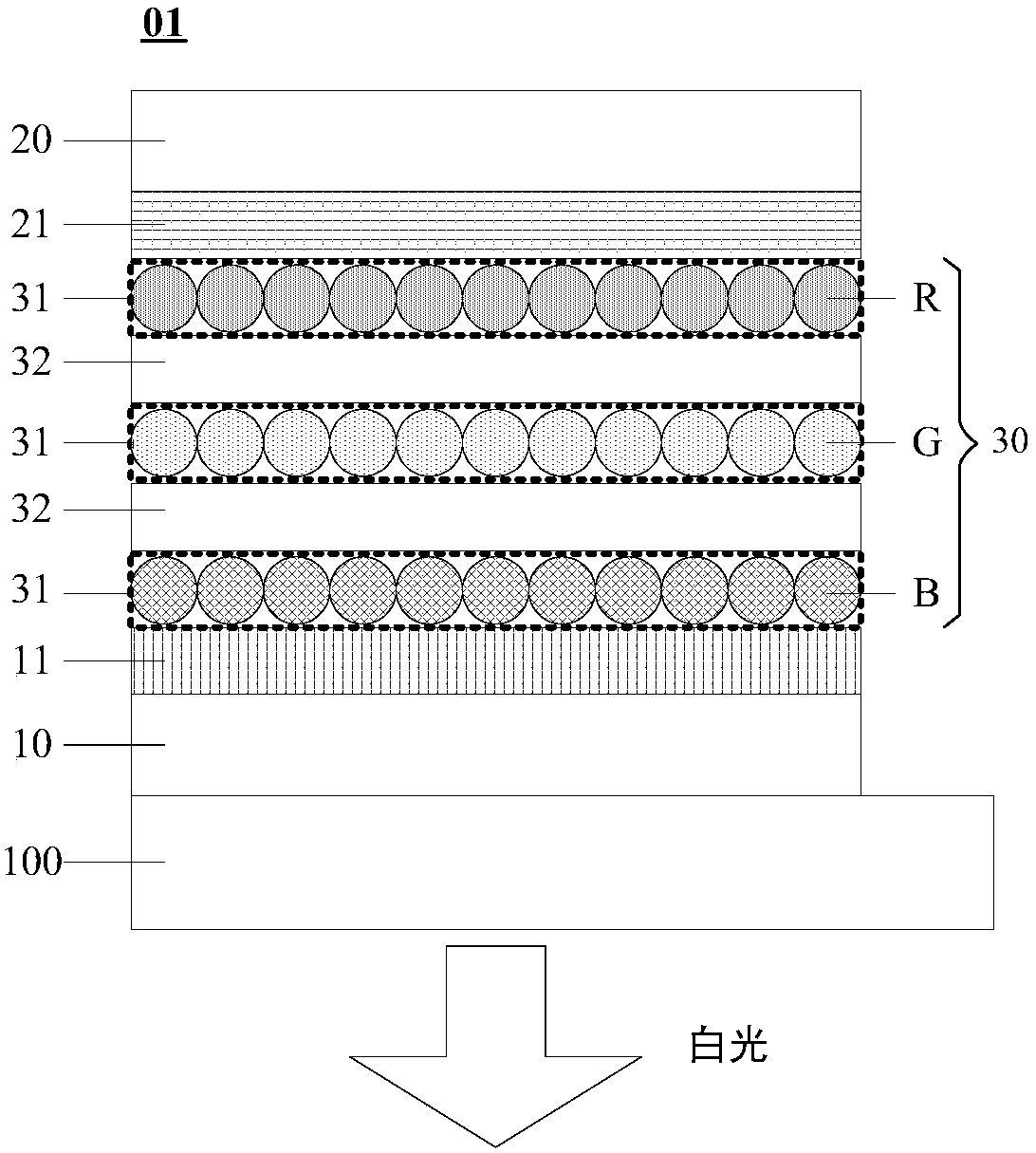
[0063] On the basis of the above, an embodiment of the present invention also provides a method for preparing the above-mentioned light-emitting device 01, the preparation method comprising: forming an anode 10, a hole transport layer 11, a light-emitting functional layer 30, and an electron transport layer 21 arranged in layers in sequence and cathode 20; wherein, the step of forming the above-mentioned luminescent functional layer 30 includes: forming at least two quantum dot luminescent layers 31 that emit light of different colors; and forming a transparent insulating layer between any adjacent two layers of quantum dot luminescent layers 31 Layer 32.
[0064] Here, the aforementioned quantum dot light-emitting layer 31 can be formed by any method of spin coating, microcontact printing, inkjet printing, and roll-to-roll printing.
[0065] Wherein, when the light-emitting device 01 is a vertical light-emitting device, that is, the anode 10 is directly formed on the substrat...
specific Embodiment 1
[0076] Embodiment 1 of the present invention provides a kind of Figure 4 The preparation method of the positive white light QLED shown, the specific steps of the preparation method are as follows:
[0077] Step S101, preparing the anode 10 on the base substrate 100;
[0078] A layer of ITO is deposited on the transparent glass substrate 100 by magnetron sputtering as a transparent anode (transmittance close to 90%), and its thickness ranges from 70 to 150 nm. Treat it with an appropriate annealing temperature to reduce its square resistance (ie, sheet resistance) to 10-40Ω / □ (the symbol "□" indicates a square).
[0079] Surface treatment is carried out to the surface of anode 10 by mechanical polishing again, so that its surface roughness Ra<2nm, Rmax<20nm; Work function (making it 4.8eV), reducing the hole injection barrier.
[0080] Step S102, forming a hole transport layer 11 on the anode 10;
[0081] The above-mentioned hole transport layer 11 can be prepared by spin ...
specific Embodiment 2
[0092] Embodiment 1 of the present invention provides a kind of Figure 5 The preparation method of the inverted white light QLED shown, the specific steps of the preparation method are as follows:
[0093] Step S201, preparing the cathode 20 on the base substrate 100;
[0094] A layer of ITO is deposited on the transparent glass substrate 100 by magnetron sputtering as a transparent cathode (transmittance close to 90%), and its thickness ranges from 70 to 150 nm. Treat it with an appropriate annealing temperature to reduce its square resistance to 10-40Ω / □.
[0095]Then the anode 10 surface is surface treated by mechanical polishing, so that its surface roughness Ra<2nm, Rmax<20nm; The work function reduces the electron injection barrier.
[0096] Step S202, forming an electron transport layer 21 on the cathode 20;
[0097] The above-mentioned electron transport layer 21 can be prepared by spin coating, coating or inkjet printing film forming process, and its thickness ra...
PUM
 Abstract
Description
Claims
Application Information