
Manufacturing method for black silicon double-face cell
A technology of a double-sided cell and a manufacturing method, which is applied in the field of solar cells, can solve the problems of hindering the progress of industrialization, cumbersome processes, and improving the power generation of solar cells, and achieves the effects of increasing power output, improving absorption, and reducing reflectivity.
- Summary
- Abstract
- Description
- Claims
- Application Information
AI Technical Summary
Problems solved by technology
Method used
Image

Examples
Embodiment
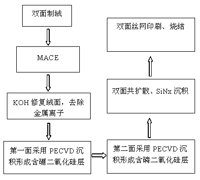
[0027] A method for manufacturing a black silicon double-sided battery, the specific steps are:
[0028] The P-type silicon chip used is 15.6cm×15.6cm, but not limited to this size; the resistivity is 1-3Ω·cm.
[0029] a. Carry out double-sided texturing of the silicon wafer;
[0030] b. Using metal-assisted catalytic etching to fabricate black silicon structures
[0031] Put the textured silicon wafer into AgNO 3 and HF mixed solution, AgNO 3 The concentration of HF is 0.001-0.2mol / L, the concentration of HF is 0.01-0.1mol / L, react at room temperature for 10-100s, after the reaction is completed, clean the silicon wafer, and then put HF and H 2 o 2 In the mixed solution, the concentration of HF is 1-5mol / L, H 2 o 2 The concentration is 0.1-2mol / L, react at room temperature for 50-200s;
[0032] c. Use acid to remove metal ions
[0033] Wash the silicon wafer obtained in step b, first react with 0.005-0.2mol / L KOH solution at 70°C for 50-200s, and then use 0.005-0.2mol...
PUM
| Property | Measurement | Unit |
|---|---|---|
| electrical resistivity | aaaaa | aaaaa |
Abstract
Description
Claims
Application Information