Etching method of silicon chip grooves for optical waveguide

An optical waveguide and groove technology, applied in the directions of light guide, optics, optical components, etc., can solve the problems of increasing the transmission loss of the optical waveguide and increasing the scattering loss of the transmitted light in the waveguide, so as to improve the sidewall morphology and reduce the transmission loss. Effect

Active Publication Date: 2016-05-18
CHINA ELECTRONICS TECH GRP NO 23 RES INST
View PDF5 Cites 11 Cited by
  • Summary
  • Abstract
  • Description
  • Claims
  • Application Information

AI Technical Summary

Problems solved by technology

However, when this process is applied to the formation of the optical waveguide of the optical device, such vertical stripes will be formed on the side wall of the waveguide

Method used


Image

  • Etching method of silicon chip grooves for optical waveguide
  • Etching method of silicon chip grooves for optical waveguide
  • Etching method of silicon chip grooves for optical waveguide

Examples


Embodiment Construction

[0028] The present invention will be further described below in conjunction with the accompanying drawings and embodiments.

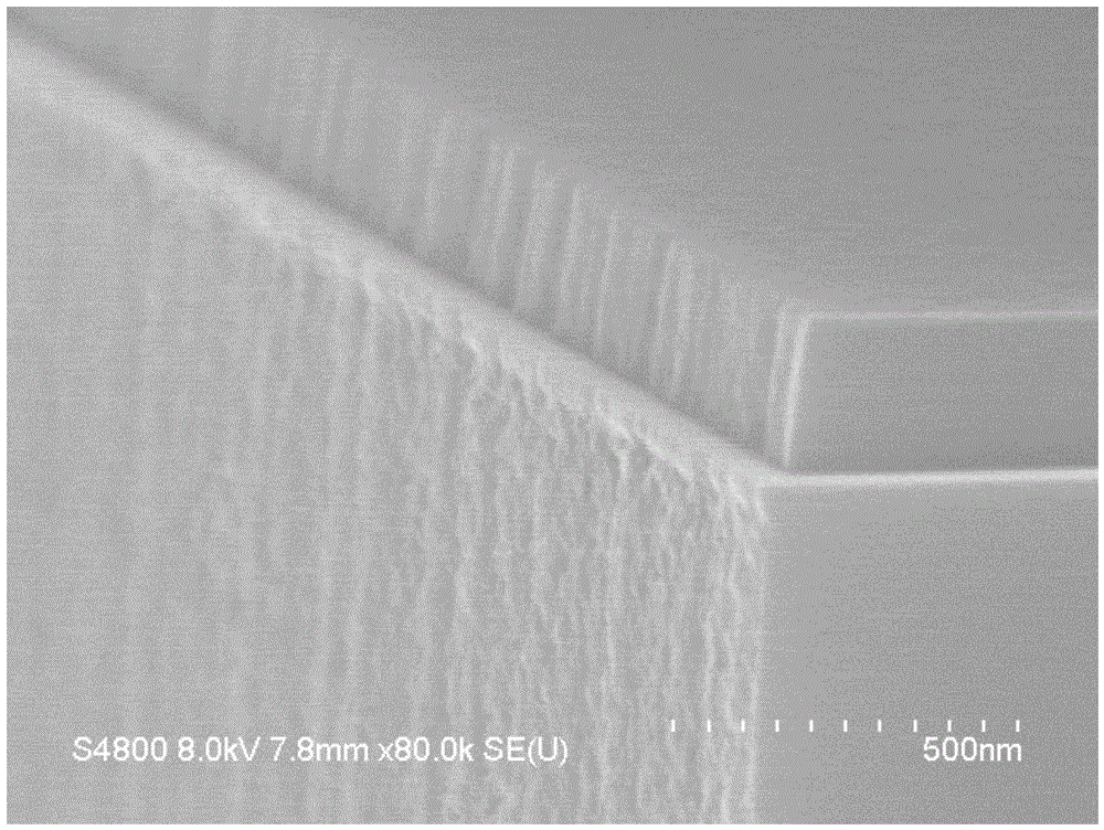
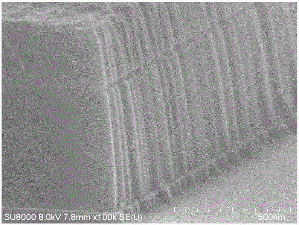
[0029] figure 1 It is a photograph of the surface topography of the existing silicon trench and the side wall of the shielding layer; figure 2 It is a photograph of the surface topography of the existing silicon trench shielding layer and the photoresist sidewall.

[0030] see figure 1 with figure 2 , analyzing the source of the stripes layer by layer, it is found that the stripes on the sidewall of the silicon trench are consistent with the stripes on the sidewall of the shielding layer silicon nitride, and are passed down from the stripes on the sidewall of the silicon nitride (or silicon oxide), and from the silicon There is a tendency for the stripes to gradually become lighter from the top to the bottom of the groove. The stripes on silicon nitride are generated when silicon nitride is etched with photoresist as a mask layer. Therefore, the ...


PUM

PropertyMeasurementUnit
Thicknessaaaaaaaaaa

Abstract

The invention discloses an etching method of silicon chip grooves for an optical waveguide. The method includes: S1: a dielectric layer and a shielding layer are deposited on the surface of a silicon substrate in sequence, the dielectric layer is a silicon oxide layer or a silicon nitride layer, and the shielding layer is a polysilicon layer or an amorphous silicon layer; S2: shielding patterns of photoresist are formed on the surface of the shielding layer by employing a silicon groove processing photoetching mask; S3: the first etching of the shielding layer is performed by employing a dry method plasma etching process; S4: the polysilicon layer or the amorphous silicon layer after the first etching is regarded as the shielding layer, and the second etching of the dielectric layer is performed; S5: the shielding patterns of the photoresist are formed on the surface of the bare silicon substrate by employing a reverse mask of the silicon groove processing photoetching mask, and the third etching is performed; and S6: the residual dielectric layer is regarded as the shielding layer for silicon etching to obtain the required silicon grooves. According to the method, the roughness of sidewalls of the silicon grooves can be greatly improved, and the scattering loss and the transmission loss of the silicon-based optical waveguide are reduced.

Description

technical field [0001] The invention relates to a method for manufacturing a semiconductor integrated circuit, in particular to a method for etching a silicon wafer groove for an optical waveguide. Background technique [0002] The advantage of making optical waveguides with silicon materials is that the core layer and the cladding layer have a high refractive index contrast, the integration degree per unit area can be made higher, and the size can be made smaller. However, the development of silicon-based photonic integration technology still faces many problems, one of which is the loss of optical waveguides. [0003] In the manufacture of semiconductor integrated circuits, it is often necessary to etch the silicon substrate, such as the STI (shallow trench isolation) isolation process of integrated circuits, deposit a thin layer of silicon oxide on the surface of the silicon wafer, and deposit a layer of silicon nitride on the silicon oxide, Coating photoresist on the su...

Claims


Application Information

Patent Timeline
IPC IPC(8): G02B6/136G02B6/138
CPCG02B6/131G02B6/132G02B6/136G02B6/138
Inventor 李冰姜剑光陈东石
Owner CHINA ELECTRONICS TECH GRP NO 23 RES INST
Why Eureka
Try Eureka