A kind of gan-based LED epitaxial structure and growth method of n-type gan structure

A technology of epitaxial structure and growth method, applied in the direction of electrical components, circuits, semiconductor devices, etc., can solve the problems of uneven lateral expansion of holes, large lattice mismatch of superlattice, insufficient electron blocking, etc., to prevent electron overflow , Reduce crystal growth dislocations and cracks, improve the effect of antistatic ability

Active Publication Date: 2018-03-13
SHANDONG INSPUR HUAGUANG OPTOELECTRONICS
View PDF6 Cites 0 Cited by
  • Summary
  • Abstract
  • Description
  • Claims
  • Application Information

AI Technical Summary

Problems solved by technology

[0008] However, in the above technology, the P-type AlGaN layer does not block enough electrons, and the horizontal expansion of holes is not uniform, resulting in low luminous efficiency, and the superlattice lattice mismatch in the P-type region is large, which easily causes epitaxial wafers to break.

Method used


Image

  • A kind of gan-based LED epitaxial structure and growth method of n-type gan structure
  • A kind of gan-based LED epitaxial structure and growth method of n-type gan structure

Examples


Embodiment 1

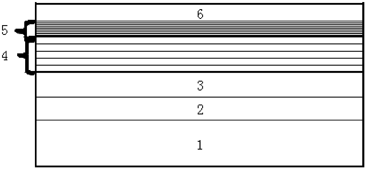
[0043] A GaN-based LED epitaxial structure with an n-type GaN structure, including a substrate layer 1, a buffer layer, an n-type structure 4, a multi-quantum well light-emitting layer 5, and a p-type structure 6 arranged sequentially from bottom to top;

[0044] The n-type structure 4 includes an n-type GaN layer with low doped Si concentration gradient, a Si-doped n-type AlGaN layer, a u-type GaN layer, and a highly Si-doped n-type GaN layer arranged in sequence from bottom to top.

[0045] The Si doping concentration of the low-doped Si concentration gradient n-type GaN layer is 5E18-2E19 / cm 3 ; The Si doping concentration of the n-type AlGaN is 5E17-5E19 / cm 3 ; The Si doping concentration of the highly doped Si n-type GaN layer is 1.5E19-5E20 / cm 3 .

[0046] The thickness of the n-type GaN layer with low-doped Si concentration gradient is 2-3 μm; the thickness of the n-type AlGaN layer is 20-60 nm; the thickness of the u-type GaN layer is 20-40 nm; the highly doped Si T...

Embodiment 2

[0051] The method for growing LED epitaxial structure as described in embodiment 1, comprises the following steps:

[0052] (1) Carry out nitriding treatment to substrate layer 1; The preferred sapphire substrate of substrate layer 1 described here, utilizes metal-organic chemical vapor deposition (MOCVD) equipment to grow on the sapphire substrate with metal-organic chemical vapor deposition, using high Pure H 2 or high purity N 2 or high purity H 2 and N 2 The mixed gas as the carrier gas, high-purity NH 3 As a N source, the reaction chamber pressure is 200mbar;

[0053] (2) A buffer layer is grown on the substrate layer 1 after nitriding treatment, that is, a nucleation layer 2 and a non-doped gallium nitride layer 3 are grown sequentially; Layer 2, thickness 20-40nm;

[0054] (3) growing the n-type structure 4 on the buffer layer includes:

[0055] a. The growth temperature of n-type GaN layer with low-doped Si concentration gradient is 1100°C, the growth pressure i...


PUM


Abstract

The invention relates to a GaN-based LED epitaxial structure and a growth method of an n-type GaN structure, including a substrate layer, a buffer layer, an n-type structure, a multi-quantum well light-emitting layer and a p-type structure arranged sequentially from bottom to top; The n-type structure includes an n-type GaN layer with a low-doped Si concentration gradient, a Si-doped n-type AlGaN layer, a u-type GaN layer, and a highly-doped Si n-type GaN layer arranged in sequence from bottom to top. The present invention adopts an n-type superlattice structure with a layer of nAlGaN inserted in the middle of a combination of high and low doping, successfully overcomes the method of blindly using high-doped nGaN to reduce the luminous voltage in the prior art, and makes a breakthrough in structural design. Based on growth experience, it was unexpectedly found that high-doped nGaN and low-doped nGaN are used to match the middle nAlGaN layer. This method can increase the electron concentration, thereby increasing the electron mobility and reducing the luminous voltage; at the same time, the growth of the n-type region determines the stability of the entire LED structure, especially parameters such as reverse voltage, antistatic ability and leakage.

Description

technical field [0001] The invention relates to a GaN-based LED epitaxy structure and a growth method with an n-type GaN structure, and belongs to the technical field of LED epitaxy design. Background technique [0002] In the early 1990s, the third-generation wide-bandgap semiconductor materials represented by nitrides made a historic breakthrough. Researchers successfully prepared blue-green and ultraviolet LEDs on gallium nitride materials, making LED lighting become possible. In 1971, the first gallium nitride LED die came out. In 1994, gallium nitride HEMTs appeared blue light GaN-based diodes with high electron mobility, and gallium nitride semiconductor materials developed very rapidly. [0003] Semiconductor light-emitting diodes have the advantages of small size, ruggedness, strong controllability of light-emitting bands, high luminous efficiency, low heat loss, low light decay, energy saving, and environmental protection. Communication and other fields have a wid...

Claims


Application Information

Patent Timeline
Patent Type & Authority Patents(China)
IPC IPC(8): H01L33/14H01L33/00
CPCH01L33/007H01L33/145
Inventor 王磊曲爽逯瑶王成新徐现刚
Owner SHANDONG INSPUR HUAGUANG OPTOELECTRONICS
Why Eureka
Try Eureka