Silica-based gallium nitride growing method based on graphene and magnetron sputtering aluminum nitride

A magnetron sputtering and growth method technology, applied in the field of electronics, can solve the problems of difficult growth, high substrate cost, poor crystal quality, etc., and achieve the effect of overcoming difficulties in nucleation, high dislocation density, and easy nucleation

Active Publication Date: 2016-06-08
XIDIAN UNIV
View PDF5 Cites 23 Cited by
  • Summary
  • Abstract
  • Description
  • Claims
  • Application Information

AI Technical Summary

Problems solved by technology

But, the weak point that this method still exists is: 1, this method adopts silicon carbide as substrate, and substrate cost is too high
2. This method directly grows graphene on the silicon carbide substrate, which is difficult to grow, and the quality

Method used


Image

  • Silica-based gallium nitride growing method based on graphene and magnetron sputtering aluminum nitride
  • Silica-based gallium nitride growing method based on graphene and magnetron sputtering aluminum nitride

Examples


Embodiment 1

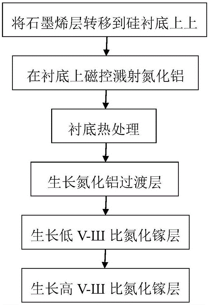
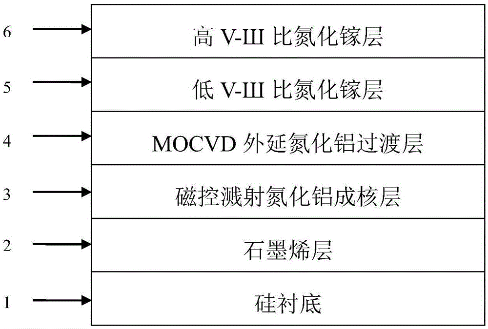
[0052] Example 1: Growth of gallium nitride on a silicon (100) substrate based on graphene and magnetron sputtering aluminum nitride.

[0053] Step 1: Transfer graphene.

[0054] Adopt chemical vapor deposition method, grow the single-layer graphene of 0.34nm on the copper substrate, then place the single-layer graphene in the mixed solution of 1M ferric chloride and 2M hydrochloric acid for 12 hours, remove the metal substrate after finally The single-layer graphene is transferred onto a silicon (100) substrate to obtain a silicon (100) substrate covered with graphene with a thickness of 0.34 nm.

[0055] Step 2: magnetron sputtering aluminum nitride.

[0056] The silicon (100) substrate covered with graphene is placed in a magnetron sputtering system, the pressure of the reaction chamber is 1Pa, nitrogen and argon are introduced into the system for 5 minutes, and aluminum with a purity of 5N is used as the target material, and radio frequency magnetron sputtering is adopted...

Embodiment 2

[0065] Example 2: Growth of gallium nitride on a silicon (111) substrate based on graphene and magnetron sputtering aluminum nitride.

[0066] Step A: Transfer graphene.

[0067] Adopt chemical vapor deposition method, grow the single-layer graphene of 0.34nm on the copper substrate, then place the single-layer graphene in the mixed solution of 1M ferric chloride and 2M hydrochloric acid for 12 hours, remove the metal substrate after finally The single-layer graphene was transferred to a silicon (111) substrate to obtain a silicon (111) substrate covered with graphene with a thickness of 0.34 nm.

[0068] Step B: magnetron sputtering aluminum nitride.

[0069] The silicon (111) substrate covered with graphene is placed in a magnetron sputtering system, the pressure of the reaction chamber is 1Pa, nitrogen and argon are introduced into the system for 5 minutes, and aluminum with a purity of 5N is used as the target material, and radio frequency magnetron sputtering is adopted....


PUM


Abstract

The invention relates to a silica-based gallium nitride growing method based on graphene and magnetron sputtering aluminum nitride. The method includes the following steps that 1, single-layer graphene is transferred to a silicon substrate through a transferring technology of graphene on a copper substrate; 2, an aluminum nitride film grows on the silicon substrate covered by the graphene layer through magnetron sputtering; 3, heat treatment is conducted; 4, an aluminum nitride film is formed in an epitaxy mode through a metal organic chemical vapor deposition (MOCVD) method; 5, a sample is put into MOCVD, and a low-V/III-ratio GaN epitaxial layer and a high V/III ratio GaN epitaxial layer are sequentially formed in an epitaxy mode. The good-quality gallium nitride epitaxial layer covering the silicon substrate of the graphene layer is obtained easily through the method.

Description

technical field [0001] The invention belongs to the field of electronic technology, and further relates to a silicon-based gallium nitride growth method based on graphene and magnetron sputtering aluminum nitride in the field of microelectronic technology. The invention can be used to grow silicon-based gallium nitride, and the obtained silicon-based gallium nitride can be further manufactured into semiconductor devices. Background technique [0002] Gallium nitride is widely used in optoelectronic devices and electronic devices due to its advantages such as large band gap, high electron mobility, and large breakdown electric field. Therefore, growing high-quality gallium nitride is the key to making microwave power devices. [0003] Silicon has an extremely mature development and application in the field of microelectronics. The single crystal of silicon has high quality, low cost, large size, and can realize photoelectric integration, so it is very suitable for preparing ...

Claims


Application Information

Patent Timeline
IPC IPC(8): H01L21/02C23C14/35C23C14/06C23C16/34C23C28/04
CPCC23C14/0617C23C14/35C23C16/303C23C28/04H01L21/02381H01L21/02458H01L21/0254H01L21/0262H01L21/02631
Inventor 张进成陈智斌吕佳骐郝跃
Owner XIDIAN UNIV
Why Eureka
Try Eureka