Polymer, composition for organic electroluminescent element, organic electroluminescent element, organic el display device, and organic el lighting
A polymer and luminescent technology, applied in the polymer field, can solve the problems of poor driving stability, difficult lamination of wet film forming methods, and has not yet reached the practical level, and achieve excellent durability, excellent hole injection, and hole The accumulation inhibitory effect of
- Summary
- Abstract
- Description
- Claims
- Application Information
AI Technical Summary
Problems solved by technology
Method used
Image
Examples
Embodiment 1
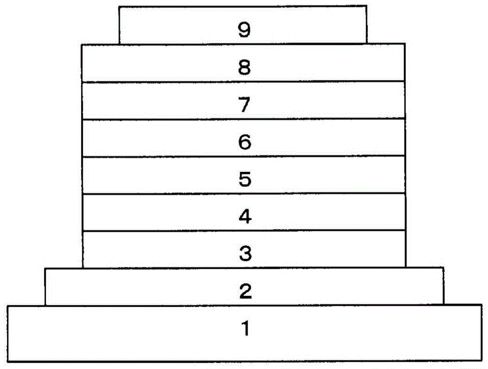
[0424] make out figure 1 The organic electroluminescence device shown.
[0425] After depositing an indium tin oxide (ITO) transparent conductive film on a glass substrate 1 by sputtering, a 2mm-wide stripe was patterned using a common photolithography technique and hydrochloric acid etching to form an anode 2 with a film thickness of 70nm. . After patterning, the ITO substrate is cleaned in the order of ultrasonic cleaning with aqueous surfactant solution, water washing with ultrapure water, ultrasonic cleaning with ultrapure water, and water washing with ultrapure water, then dried with compressed air, and finally UV ozone cleaning.
[0426] Next, prepare the arylamine polymer containing the following structural formula (P1), 4-isopropyl-4'-methyldiphenyliodonium tetrakis(pentafluorophenyl) boron represented by the structural formula (A1) A coating solution for forming a hole injection layer of acid salt and ethyl benzoate. This coating solution was formed into a film on...
Embodiment 2
[0469] For the hole transport layer 4, a coating solution for forming a hole transport layer containing a polymer 2 (P4) represented by the following structural formula was prepared, and formed on the hole injection layer 3 by spin coating under the following conditions. The film was heated to form a hole transport layer with a film thickness of 20 nm.
[0470]
[0471]
[0472] Solvent cyclohexylbenzene
[0473] Coating solution concentration 1.5% by weight
[0474]
[0475]
[0476] For the light-emitting layer 5, a coating solution for forming a light-emitting layer containing compounds (H3) and (D2) represented by the following structural formulas was prepared, and a film was formed by spin coating under the following conditions, and heating was performed. On the layer 4, a light emitting layer with a film thickness of 41 nm was formed.
[0477] Except for this, an organic electroluminescent element was produced in the same manner as in Example 1. Table 10 sho...
Embodiment 3
[0500] The hole mobility of polymer 3 (P6) was measured using the time-of-flight (TOF) method in the same manner as the method described in JP-A-2014-51667.
[0501]
[0502] First, an ITO transparent conductive film (ITO stripes) was deposited on a glass substrate with a thickness of 70 nm, and the resulting substrate (manufactured by GEOMATEC) was subjected to ultrasonic cleaning with an aqueous surfactant solution, water washing with ultrapure water, ultrapure water After cleaning in the order of ultrasonic cleaning with pure water and water washing with ultrapure water, drying with compressed air was performed, and ultraviolet ozone cleaning was performed thereafter.
[0503] A solution was prepared by dissolving (P6) at a concentration of 10% by mass in a solvent mixed with toluene and silicone oil (manufactured by Shin-Etsu Silicones: KF-96), and formed on the cleaned substrate by spin coating. membrane. It should be noted that all film formation was performed in a n...
PUM
| Property | Measurement | Unit |
|---|---|---|
| Film thickness | aaaaa | aaaaa |
| Film thickness | aaaaa | aaaaa |
| Film thickness | aaaaa | aaaaa |
Abstract
Description
Claims
Application Information


