Epitaxial growth method for increasing p-type doping concentration of nitride light-emitting diodes

A technology for light-emitting diodes and epitaxial growth, which is applied in the fields of nanotechnology, electrical components, and nanotechnology for materials and surface science. It can solve problems such as difficulty in achieving hole concentration, difficulty in obtaining N materials, and difficulty in obtaining high hole concentration , to reduce self-compensation effect, improve crystal quality and reduce self-compensation effect

Active Publication Date: 2017-12-08
XIAMEN CHANGELIGHT CO LTD
View PDF13 Cites 0 Cited by
  • Summary
  • Abstract
  • Description
  • Claims
  • Application Information

AI Technical Summary

Problems solved by technology

However, due to the low solubility of acceptor dopants, the self-compensation effect caused by defects and the Al X Ga 1-X The high Mg acceptor activation energy in N materials makes P-Al with high hole concentration X Ga 1-X N materials have been difficult to obtain
By optimizing the epitaxial growth temperature, pressure, and rate, the hole concentration can be increased to a certain extent. In addition, the technology of energy band modulation through the growth material superlattice structure can also increase the hole concentration to a certain extent, but the existing Doping technology, it is still difficult to achieve a higher hole concentration
[0004] Currently P-Al X Ga 1-X The growth of N generally adopts uniform Mg doping technology, that is, simultaneously injecting TMGa / TMAl / NH into the reaction chamber 3 / Cp 2 Mg conducts the entire P-Al X Ga 1-X The growth of N layer, this growth process is difficult to obtain P-Al with high hole concentration X Ga 1-X The N layer restricts the improvement of the optoelectronic performance of the device

Method used


Image

  • Epitaxial growth method for increasing p-type doping concentration of nitride light-emitting diodes
  • Epitaxial growth method for increasing p-type doping concentration of nitride light-emitting diodes

Examples


Embodiment Construction

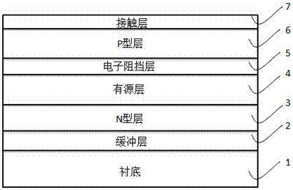
[0031] A method for epitaxial growth of a nitride light-emitting diode that can increase the P-type doping concentration, such as figure 1 As shown: a buffer layer 2 , an N-type layer 3 , a light-emitting active layer 4 , an electron blocking layer 5 , a P-type layer 6 and a contact layer 7 are grown sequentially on a substrate 1 .

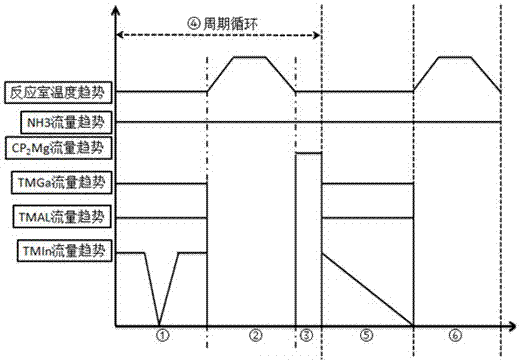
[0032] Wherein the P-type layer 6 is Al X Ga 1-X N floor, the whole production except in N 2 and ammonia (NH 3 ) atmosphere, and if figure 2 As shown, the specific growth method of this layer is as follows:

[0033] 1. Introduce ammonia gas (NH 3 ), trimethylgallium (TMGa), trimethylaluminum (TMAl), grow a layer of Al X Ga 1-XN thin layer, the growth thickness is 5-25nm, and the growth temperature is 900°C-1100°C.

[0034] During the growth process of this layer, a small amount of trimethylindium (TMIn) is also introduced: the flow rate of trimethylindium (TMIn) in this stage is the same uniform flow rate first and last, and in the middle...


PUM

PropertyMeasurementUnit
thicknessaaaaaaaaaa

Abstract

An epitaxial growth method for improving P-type doping concentration of a nitride light emitting diode relates to the technical field of nitride epitaxy. A buffer layer, an N-type layer, a light emitting active layer, an electron blocking layer, a P-type layer and a contact layer are sequentially grown on a substrate, the epitaxial growth method is characterized in that the P-type layer is formed through layered growth by controlling the flow of trimethyl indium under the atmosphere of N2 and ammonia gas, the hole concentration of a P-Al<X>Ga<1-X>N material layer can be obviously improved, the square resistance can be obviously reduced, and the light emitting diode (LED) photoelectric property based on the material layer can be obviously improved.

Description

technical field [0001] The invention relates to the technical field of nitride epitaxy, and in particular provides an epitaxial growth method capable of significantly increasing the P-type doping concentration of a nitride light-emitting diode (LED). Background technique [0002] Group III nitride materials have received extensive attention in recent years due to their broad application prospects in optoelectronics and microelectronics. Especially in the field of optoelectronics, it has been widely used to make light-emitting diodes (LEDs). With its unique advantages such as small size, long life, energy saving and environmental protection, LED plays an important role in the fields of visible light and invisible light. However with Al X Ga 1-X The P-type doping technology of nitride light-emitting materials dominated by N (1≥X≥0) has been difficult to break through, and the P-type nitride light-emitting materials with high hole concentration have been difficult to obtain,...

Claims


Application Information

Patent Timeline
Patent Type & Authority Patents(China)
IPC IPC(8): H01L33/00H01L21/02B82Y30/00B82Y40/00
CPCB82Y30/00B82Y40/00H01L21/0254H01L21/02584H01L33/0075
Inventor 卓祥景陈凯轩张永林志伟姜伟方天足刘碧霞
Owner XIAMEN CHANGELIGHT CO LTD
Why Eureka
Try Eureka