Silicon substrate nitride ultraviolet LED chip structure and implementation method therefor

A technology of LED chips and implementation methods, applied in electrical components, circuits, semiconductor devices, etc., can solve the problems of poor heat dissipation of ultraviolet LED chips, expensive AlN substrates, and difficult to achieve commercialization, and achieves suitable for large-scale production. Good electrical and thermal conductivity, the effect of reducing absorption

Active Publication Date: 2016-06-29
晶能光電股份有限公司
View PDF7 Cites 5 Cited by
  • Summary
  • Abstract
  • Description
  • Claims
  • Application Information

AI Technical Summary

Problems solved by technology

Due to the insulating properties of the sapphire substrate itself and poor thermal conductivity, the existing LED products have the following disadvantages: (1) the UV LED chip based on the horizontal structure of the sapphire substrate does not dissipate heat well, and the GaN (nitrided) in the epitaxial layer Gallium) easily absorbs the ultraviolet light in the active area, and is only suitable for small-sized low-power chips, and is not suitable for use under high-power conditions, such as photocuring; (2) In the p

Method used


Image

  • Silicon substrate nitride ultraviolet LED chip structure and implementation method therefor
  • Silicon substrate nitride ultraviolet LED chip structure and implementation method therefor
  • Silicon substrate nitride ultraviolet LED chip structure and implementation method therefor

Examples


specific Embodiment 1

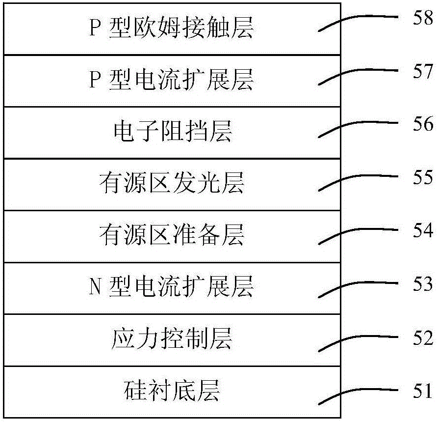
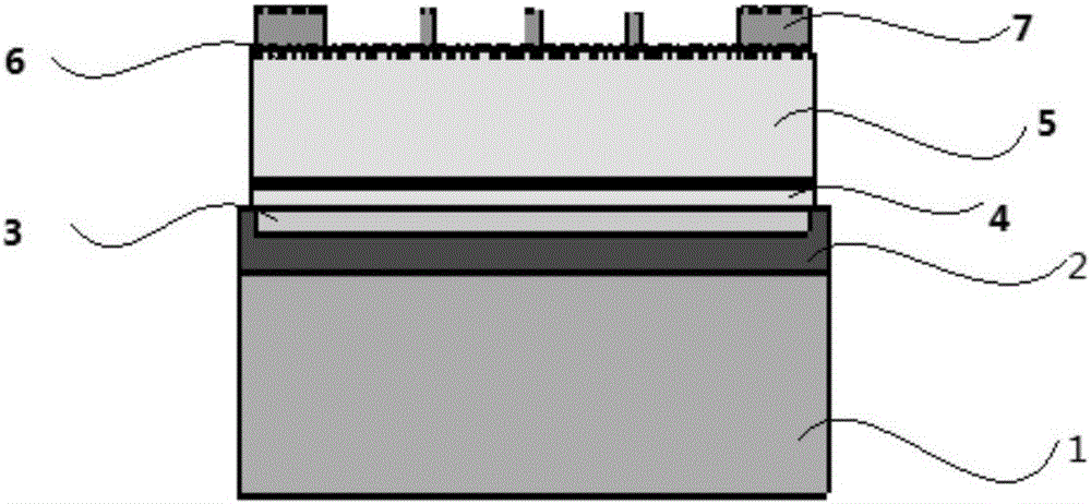
[0059] Based on the silicon-substrate ultraviolet LED epitaxial structure provided by the present invention, a silicon-substrate ultraviolet light-emitting diode chip structure is prepared in this embodiment. The structure is shown in FIG. 3 , and the preparation process includes the following steps: as shown in FIG. 3 .

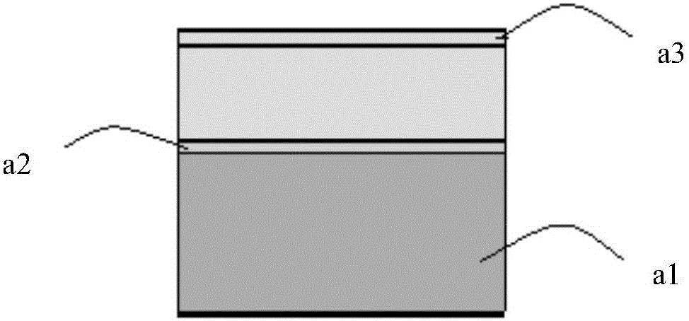
[0060] Such as Figure 3a First, the surface layer of the silicon substrate ultraviolet LED epitaxial structure, that is, the p-type ohmic contact layer a3, is surface-cleaned with acetone and alcohol, and then it is surface-treated with sulfuric acid: hydrogen peroxide: water = 1:1:3 to ensure that the surface is free of any impurities. Next, Mg activation annealing is carried out on the epitaxial structure whose surface has been cleaned. The annealing conditions are: at 550°C, N 2 :O 2 Anneal for 3 minutes (minutes) in an environment with a ratio of 4:1. In addition, in Figure 3a Among them, a1 is the silicon substrate layer, a2 is the stress control ...


PUM

PropertyMeasurementUnit
Thicknessaaaaaaaaaa
Thicknessaaaaaaaaaa
Thicknessaaaaaaaaaa

Abstract

The invention provides a silicon substrate nitride ultraviolet LED chip structure and an implementation method therefor. The preparation method for the LED chip comprises the steps of preparing an epitaxial structure, wherein the epitaxial structure comprises a growth substrate and a stress control layer; performing surface treatment on the epitaxial structure; depositing a reflective layer on the epitaxial structure and performing patterning treatment on the reflective layer; depositing a bonding layer on the patterned reflective layer; enabling the epitaxial structure after the bonding layer is deposited to be bonded with a supporting substrate through a bonding technology; removing the growth substrate and the stress control layer; roughening the stress control layer to form a roughened layer; and manufacturing grids used for electric conduction and a negative electrode bonding pad on the surface of the roughened layer to finish the preparation of the silicon substrate nitride ultraviolet LED chip structure. The ultraviolet LED epitaxial structure is growing on the high-thermal-conductivity silicon substrate, and the silicon substrate ultraviolet LED perpendicular structured chip is prepared, so that the LED chip structure has the advantages of high thermal dissipation, high chip yield and low cost.

Description

technical field [0001] The invention relates to the field of semiconductor optoelectronics, in particular to an LED chip structure and a realization method thereof. Background technique [0002] Compared with traditional ultraviolet mercury lamps, nitride ultraviolet LEDs (Light Emitting Diodes, light emitting diodes) have many advantages such as energy saving, environmental protection, long life, and good compactness. It has broad application prospects. [0003] Existing UV LEDs are generally UV LED products based on sapphire substrates. Due to the insulating properties of the sapphire substrate itself and poor thermal conductivity, the existing LED products have the following disadvantages: (1) the UV LED chip based on the horizontal structure of the sapphire substrate does not dissipate heat well, and the GaN (nitrided) in the epitaxial layer Gallium) easily absorbs the ultraviolet light in the active area, and is only suitable for small-sized low-power chips, and is no...

Claims


Application Information

Patent Timeline
IPC IPC(8): H01L33/00H01L33/02H01L33/46
CPCH01L33/0054H01L33/02H01L33/46
Inventor 刘乐功李增成鲁德孙钱赵汉民
Owner 晶能光電股份有限公司
Why Eureka
Try Eureka