Low-temperature poly-crystal thin film transistor and preparation method thereof

A thin-film transistor and low-temperature polysilicon technology, applied in transistors, semiconductor/solid-state device manufacturing, semiconductor devices, etc., can solve the problems of increasing process complexity, high manufacturing cost, low production efficiency, etc. The effect of reducing the requirements for pulse energy stability and beam fluence uniformity

Active Publication Date: 2016-07-06
TRULY HUIZHOU SMART DISPLAY
View PDF4 Cites 4 Cited by
  • Summary
  • Abstract
  • Description
  • Claims
  • Application Information

AI Technical Summary

Problems solved by technology

It needs to go through a process of photoresist coating, mask exposure, development and etching, which increases the complexity of the process, high manufacturing cost and low production efficiency

Method used


Image

  • Low-temperature poly-crystal thin film transistor and preparation method thereof
  • Low-temperature poly-crystal thin film transistor and preparation method thereof
  • Low-temperature poly-crystal thin film transistor and preparation method thereof

Examples


preparation example Construction

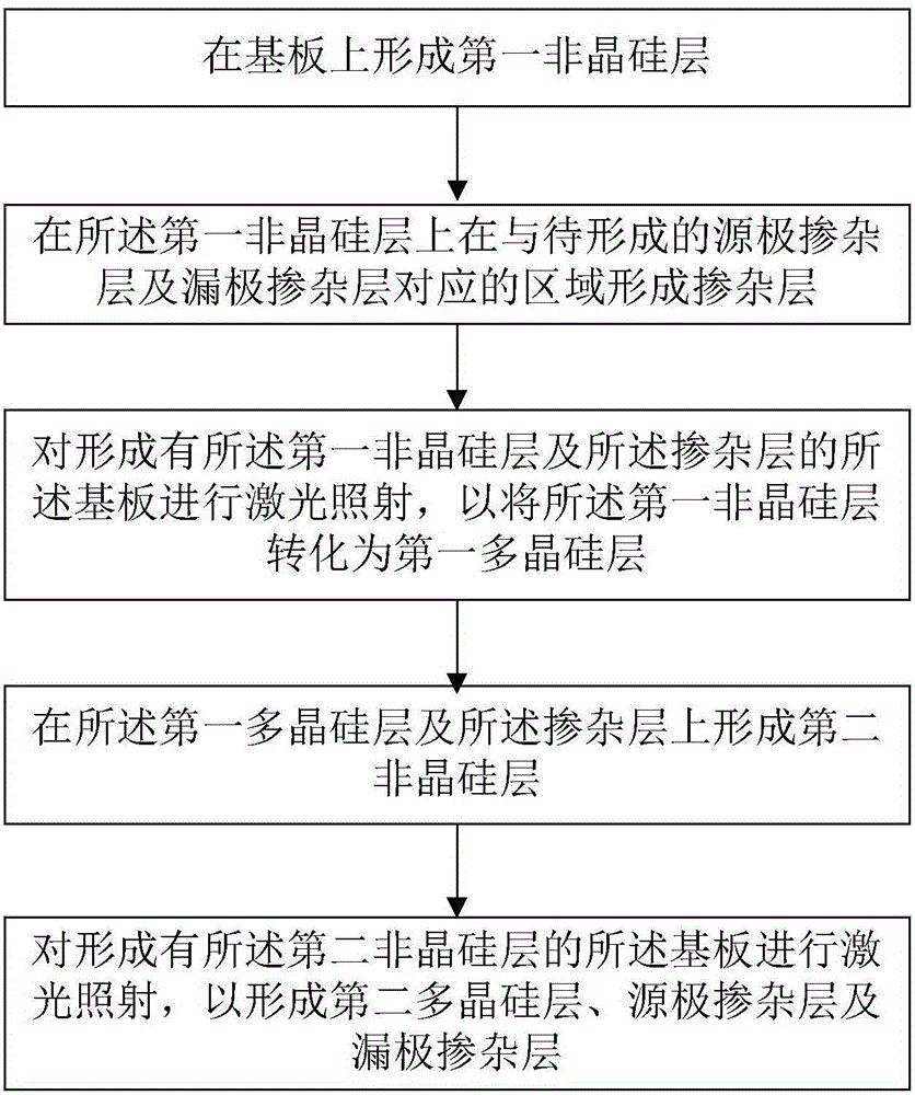
[0036] see figure 1 , which is a method for preparing a low-temperature polysilicon thin film transistor according to an embodiment of the present invention, comprising the following steps:

[0037] S110, forming a first amorphous silicon layer on the substrate;

[0038] Specifically, the thickness of the first amorphous silicon layer is 10-20 nm. Preferably, the thickness of the first amorphous silicon layer is 15 nm.

[0039] S120, forming a doped layer on the first amorphous silicon layer in regions corresponding to the to-be-formed source doped layer and drain doped layer;

[0040] In an embodiment of the present invention, a phosphorus-containing structural layer or a boron-containing structural layer is formed on the first amorphous silicon layer; a patterning process is performed on the phosphorus-containing structural layer or boron-containing structural layer, and the first amorphous silicon layer is retained. The phosphorus-containing structure layer or the boron-...


PUM


Abstract

A preparation method of a low-temperature poly-silicon thin film transistor comprises the following steps of forming a first amorphous-silicon layer on a substrate; forming doping layers on regions, corresponding to a source doping layer and a drain doping layer to be formed, on the first amorphous-silicon layer; carrying out laser irradiation on the substrate formed with the first amorphous-silicon layer and the doping layers so as to convert the first amorphous-silicon layer to a first poly-silicon layer; forming a second amorphous-silicon layer on the first amorphous-silicon layer and the doping layers; and carrying out laser irradiation on the substrate formed with the second amorphous-silicon layer to form a second poly-silicon layer, the source doping layer and the drain doping layer. According to the preparation method of the low-temperature poly-silicon thin film transistor, the first poly-silicon layer also can be taken as a second amorphous-silicon thin film to be converted into a grain structure induction layer of the poly-silicon layers, the requirements of excimer laser pulse energy stability and light beam energy density uniformity during preparation of the low-temperature poly-silicon thin film can be effectively reduced, and the problem of non-uniform display caused by laser annealing processing can be effectively solved.

Description

technical field [0001] The invention relates to the technical field of transistor manufacturing, in particular to a low-temperature polysilicon thin film transistor and a preparation method thereof. Background technique [0002] Polycrystalline silicon (p-Si) thin film has a high carrier mobility much higher than that of amorphous silicon (a-Si) and comparable to that of single crystal silicon, and is often used instead of amorphous silicon in the active layer, and thus have very important applications in integrated peripheral-driven active liquid crystal displays (AMLCDs) and active organic light-emitting diodes (AMOLEDs). The substrate of the polysilicon thin film of the flat panel display is glass which is difficult to withstand the high temperature process. Under the constraints of this condition, the low temperature polysilicon (LTPS) technology is an inevitable choice for the industry. [0003] At present, the most widely used polysilicon film crystallization method i...

Claims


Application Information

Patent Timeline
Patent Type & Authority Applications(China)
IPC IPC(8): H01L29/786H01L21/336H01L21/263H01L21/225
CPCH01L21/225H01L21/263H01L29/66757H01L29/78675
Inventor 陈卓陈建荣任思雨苏君海李建华
Owner TRULY HUIZHOU SMART DISPLAY
Why Eureka
Try Eureka