AlGaInP light-emitting diode

A technology of light-emitting diodes and light-emitting layers, applied in semiconductor devices, electrical components, circuits, etc., can solve the problems of inability to meet market demand, deterioration of anti-aging performance under high current, etc., to improve current expansion, improve aging performance, and improve reliability. performance effect

Active Publication Date: 2016-07-06
XIAMEN SANAN OPTOELECTRONICS TECH CO LTD
View PDF9 Cites 7 Cited by
  • Summary
  • Abstract
  • Description
  • Claims
  • Application Information

AI Technical Summary

Problems solved by technology

When the chip area is reduced, for example, when the chip size is 7.0mil*7.0mil, the anti-aging performance of the traditional LED structure will be significantly worse, which cannot meet the market demand.

Method used


Image

  • AlGaInP light-emitting diode
  • AlGaInP light-emitting diode
  • AlGaInP light-emitting diode

Examples


Embodiment 1

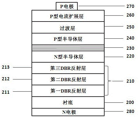
[0037] Such as figure 2As shown, this embodiment provides an AlGaInP light-emitting diode, including the following process steps: using metal organic chemical vapor deposition (MOCVD) to sequentially epitaxially grow a first DBR reflective layer 211, a second DBR reflective layer 212, and a second DBR reflective layer 212 on a substrate 200. Three DBR reflective layer 213 , N-type semiconductor layer 220 , quantum well light-emitting layer 230 , P-type semiconductor layer 240 , transition layer 250 and P-type current spreading layer 260 .

[0038] The manufacturing process of the AlGaInP light-emitting diode described in the present invention uses high-purity hydrogen (H2) as the carrier gas, trimethylgallium (TMGa), trimethylaluminum (TMAl), trimethylindium (TMIn), arsine ( AsH3), phosphine (PH3) are respectively used as sources of Ga, Al, In, As, and P, and silane (Si2H6) and dimagnesium (Cp2Mg) are used as N and P-type dopants respectively. The specific method is describe...

Embodiment 2

[0050] Such as figure 2 As shown, the difference between Embodiment 2 and Embodiment 1 is that the doping concentration of the multispectral DBR is increased, and the doping concentration of the three-stage DBR is increased by 20% respectively. That is: the doping concentration of the first DBR reflective layer 211 is 2.4×10 19 cm -3 , the doping concentration of the second DBR reflective layer 212 is 1.2×10 19 cm -3 , the doping concentration of the third DBR reflective layer 213 is 7.2×10 18 cm -3 , and the rest of the structure remains unchanged.

[0051] The new AlGaInP structure LED, after preparing the P-type electrode 270 and the N-type electrode 280, is evaluated with a small-sized chip of 5.8mil*5.8mil. At 100mA and a high temperature of 50°C, the long-term aging light decay value can be controlled at minus 5%. within. It can be seen that by increasing the DBR doping concentration, the high current resistance performance of small-sized chips can be significant...

Embodiment 3

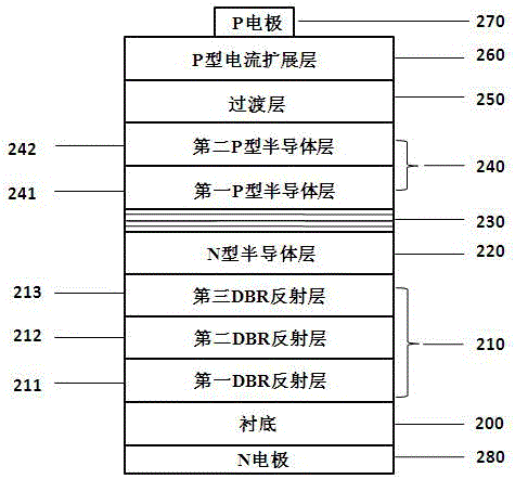
[0053] The difference between Embodiment 3 and Embodiment 2 lies in that on the basis of Embodiment 2, the doping concentration of the second P-type semiconductor layer adjacent to the transition layer is reduced to prepare a segmented doped P-type semiconductor layer. Such as image 3 As shown, grow a P-type semiconductor layer on the 230 quantum well light-emitting layer, preferably Al x In (1-x) p. The growth temperature was adjusted to 670 degrees, the pressure of the reaction chamber was set to 60 Torr, and Mg was selected for doping. When growing the first P-type semiconductor layer 241 adjacent to the quantum well light-emitting layer, Cp2Mg needs to be introduced, and the flow setting should be kept constant for 10 minutes, with a doping concentration of 1.0×10 18 cm -3 , the growth thickness is about 0.5 μm. Next, when growing the second P-type semiconductor layer 242 adjacent to the transition layer, it is necessary to use a 1min gradual change method to reduce ...


PUM


Abstract

The invention provides an AlGaInP light-emitting diode, which sequentially comprises a substrate, a DBR reflecting layer, an N-type semiconductor layer, a quantum well light-emitting layer, a P-type semiconductor layer, a transition layer and a P-type current diffusion layer from bottom to top, wherein multi-spectral doping is adopted by the DBR reflecting layer; the P-type semiconductor layer comprises a first P-type semiconductor layer and a second P-type semiconductor layer; the first P-type semiconductor layer is adjacent to the quantum well light-emitting layer; the second P-type semiconductor layer is adjacent to the transition layer; and the doping concentration of the second P-type semiconductor layer is smaller than that of the first P-type semiconductor layer. Diffusion of a current in the DBR reflecting layer is facilitated by improving the multi-spectral DBR doping concentration; the ageing property is improved; a concentration difference is formed by the P-type semiconductor doped layer and the transition layer for balancing doping of the transition layer by lowering the P-type semiconductor doped layer adjacent to the transition layer; light attenuation caused by nonradiative recombination increase introduced by high doping of the transition layer in long-term ageing is avoided; and the ageing property is further improved.

Description

technical field [0001] The invention relates to the field of semiconductor optoelectronic devices, in particular to an AlGaInP light-emitting diode with improved high-current aging resistance. Background technique [0002] In recent years, various methods have been developed to improve the brightness of AlGaInP series light-emitting diodes (Light Emitting Diode, LED for short), and breakthroughs have been made, making them widely used in display systems, lighting systems, automotive systems and other fields. For example: Chinese Patent No. 201210341574.6 proposes to have at least two Bragg reflective layers corresponding to different emission wavelengths to expand the bandwidth of reflected wavelengths in LEDs and improve internal quantum efficiency. However, in the fierce market competition, in order to reduce the cost, people continue to shrink the chip size, but other performance problems are derived. When the chip area is reduced, for example, when the chip size is 7.0m...

Claims


Application Information

Patent Timeline
Patent Type & Authority Applications(China)
IPC IPC(8): H01L33/06H01L33/26
CPCH01L33/06H01L33/305H01L33/10H01L33/04H01L33/0066H01L33/14
Inventor 郑元宇郑建森伍明跃周启伦邱财华罗宵林峰李水清吴超瑜蔡坤煌
Owner XIAMEN SANAN OPTOELECTRONICS TECH CO LTD
Why Eureka
Try Eureka