
Preparation method for large-area homogeneous organic-inorganic perovskite thin film and product and application of large-area homogeneous organic-inorganic perovskite thin film

A large-area, inorganic calcium technology, applied in the field of solar cells, can solve the problems of poor uniformity of perovskite film coverage, limitation of perovskite film preparation, waste of raw materials, etc., and achieve the goal of overcoming poor coverage uniformity, saving raw materials, and low cost Effect

Active Publication Date: 2016-07-20
HANGZHOU ZHONGNENG PHOTOELECTRIC TECH CO LTD
View PDF3 Cites 8 Cited by
  • Summary
  • Abstract
  • Description
  • Claims
  • Application Information

AI Technical Summary

Problems solved by technology

At present, the solution spin coating method is generally used to prepare perovskite films, but the perovskite films prepared by this method have poor coverage uniformity, low repeatability, and waste of raw materials, which greatly limits the preparation of large-area perovskite films.

Method used


Image

  • Preparation method for large-area homogeneous organic-inorganic perovskite thin film and product and application of large-area homogeneous organic-inorganic perovskite thin film
  • Preparation method for large-area homogeneous organic-inorganic perovskite thin film and product and application of large-area homogeneous organic-inorganic perovskite thin film
  • Preparation method for large-area homogeneous organic-inorganic perovskite thin film and product and application of large-area homogeneous organic-inorganic perovskite thin film

Examples


preparation example Construction

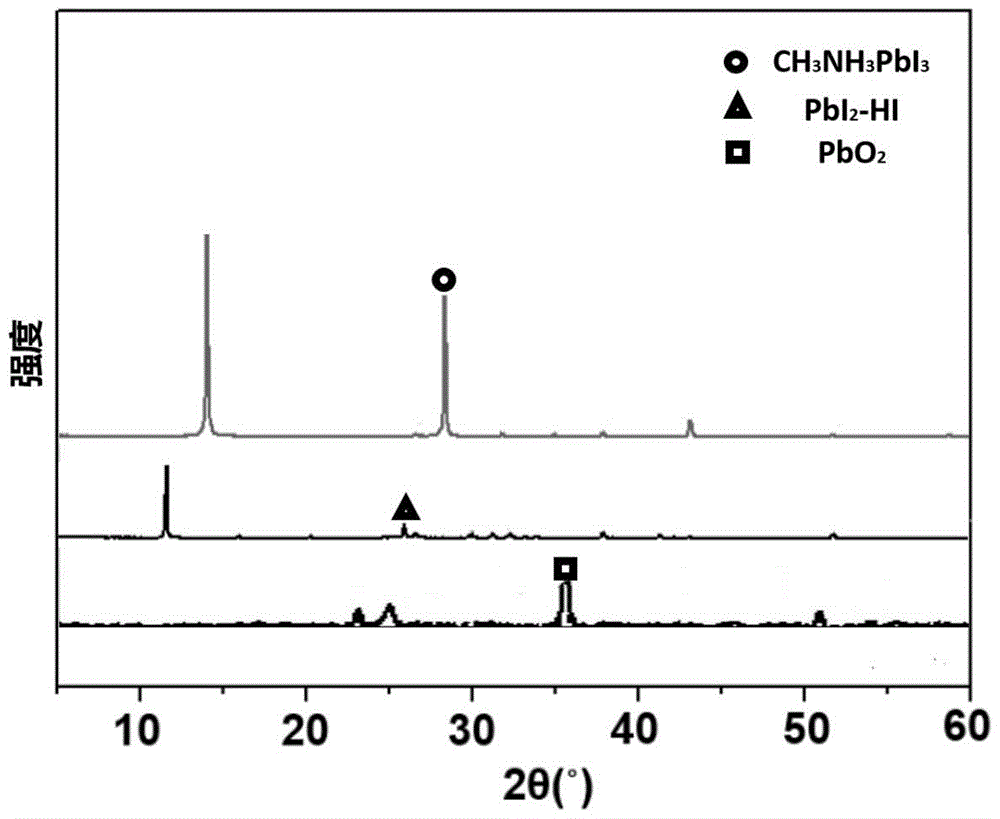
[0027] As mentioned above, the present invention provides a method for preparing a large-area homogeneous organic-inorganic perovskite film, such as figure 1 As shown, it comprises the following steps: 1) preparing lead-containing compound slurry; 2) setting a conductive substrate, and screen-printing the lead-containing compound slurry on it, and obtaining uniform lead oxide on the conductive substrate after sintering Thin film; 3) Put the lead oxide thin film obtained in step 2) into the first steam and the second steam and fumigate sequentially to prepare a large-area homogeneous organic-inorganic perovskite thin film.

[0028] What the method of the present invention prepares is a kind of large-area homogeneous organic-inorganic perovskite thin film, and described large area refers to that the area of ​​described thin film is controllable in a large range, and this is caused by the characteristic of screen printing decided. Specifically, the screen printing technology det...

Embodiment 1

[0041] The present invention according to figure 1 The process shown prepares a large-area homogeneous organic-inorganic perovskite film, and the specific preparation steps are as follows:

[0042] 1) Preparation of PbO 2 Nanoparticles: PbO with a diameter of 5-100nm is synthesized by a solid-state chemical reaction method 2 nanoparticles.

[0043] 2)PbO 2 Preparation of conductive paste:

[0044] First weigh PbO with a diameter of 5-100nm in proportion 2 Nanoparticles and additives terpineol and ethyl cellulose, of which, PbO 2 The mass ratio of nanoparticles to additives is 1:4 to 1:15, and the PbO 2 Nanoparticles and additives were dissolved in an appropriate amount of absolute ethanol, then stirred for 30 minutes, ultrasonically crushed for 5 to 10 minutes, repeated 3 to 8 times, and then the dispersed PbO 2 The solution is ball milled for 5-20 hours, and finally the PbO is taken out 2 The dispersion was then rotary evaporated for 20 to 120 minutes to remove ethano...

Embodiment 2 and comparative example 1

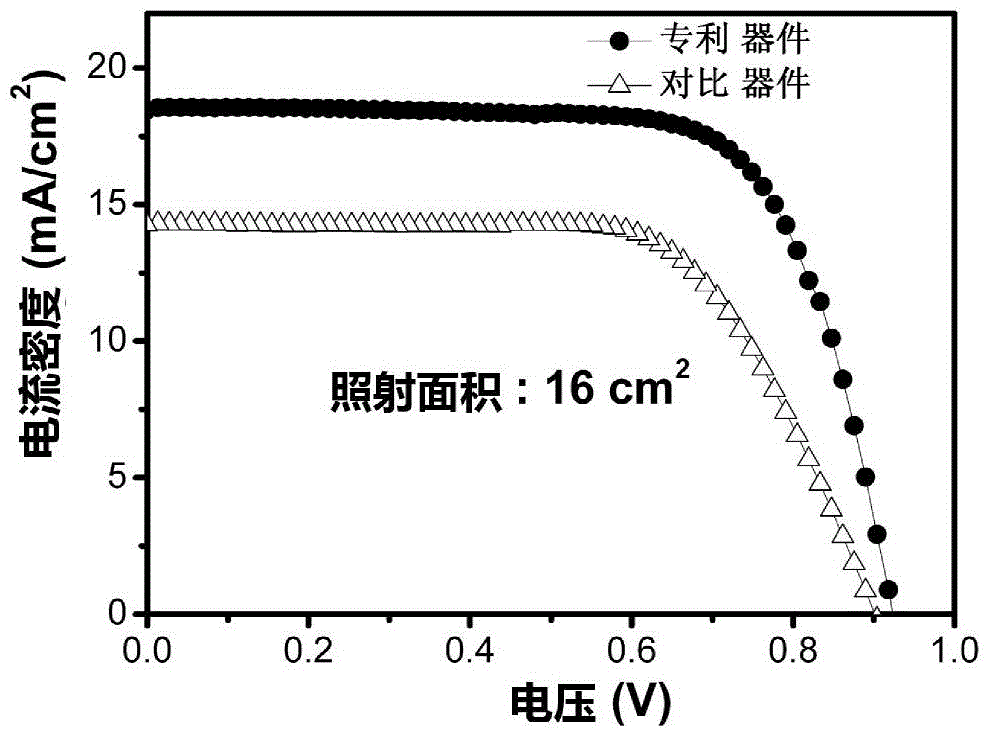
[0053] In order to show the advantages of preparing large-area homogeneous perovskite films more intuitively, a perovskite solar cell with p-i-n structure is provided below, from bottom to top are FTO transparent conductive glass, NiO dense layer, light harvesting layer (the perovskite film in embodiment 1 or the perovskite film in the prior art), Zn 2 SnO 4 Electron transport layer and metal electrode, specific implementation steps are:

[0054] Step S1) Substrate preparation: ultrasonically clean the FTO transparent conductive glass with deionized water, ethanol and acetone in sequence, and then treat it with ultraviolet and ozone for 15-30 minutes, and set aside;

[0055] Step S2) Preparation of the NiO dense layer: pre-preparing nickel acetylacetonate acetonitrile solution at a ratio of 1:10-100, preheating the clean FTO transparent conductive glass substrate at 400-600°C, and then pre-preparing the acetylacetonate Acetone-nickel-acetonitrile solution is sprayed on the s...


PUM

PropertyMeasurementUnit
diameteraaaaaaaaaa
thicknessaaaaaaaaaa
thicknessaaaaaaaaaa

Abstract

The invention relates to a preparation method for a large-area homogeneous organic-inorganic perovskite thin film and a product and application of the large-area homogeneous organic-inorganic perovskite thin film. The method comprises the following steps of 1) preparing lead-containing compound paste; 2) arranging a conductive substrate, silk-screen printing the lead-containing compound paste on the conductive substrate, and sintering the conductive substrate to obtain a uniform lead oxide thin film on the conductive substrate; and 3) respectively placing the lead oxide thin film in first steam and second steam for fumigation to prepare the uniform perovskite thin film. According to the method, a lead oxide precursor is prepared by a silk-screen printing method, and the homogeneous organic-inorganic perovskite thin film with high uniformity and controllable area is obtained by a series of simple fumigation chemical processing; and moreover, the process is simple, the repetitive rate is high, the cost is low, raw material is saved, and a large-area solar cell device with excellent and stable performance can be acquired.

Description

technical field [0001] The invention belongs to the technical field of solar cells, and in particular relates to a perovskite thin film, a perovskite solar cell containing the same and a preparation method thereof. Background technique [0002] Solar energy is an inexhaustible renewable clean energy with unique advantages and huge development potential. The large-scale development and utilization of solar energy is of great significance for establishing a reasonable green energy structure and achieving the goal of maximum energy conservation and emission reduction. Currently, the relatively mature photovoltaic technologies in the market include the first-generation silicon-based semiconductor solar cells and the second-generation CIGS, CdTe and other multi-component thin-film solar cells. Although the annual growth rate is 30%, the total installed power generation is still insufficient. 1% of total global energy consumption. In addition, the materials of silicon-based semi...

Claims


Application Information

Patent Timeline
Patent Type & Authority Applications(China)
IPC IPC(8): H01L51/44H01L51/42H01L51/48
CPCH10K71/00H10K71/13H10K30/00H10K30/80H10K30/87H10K2102/00Y02E10/549Y02P70/50
Inventor 石磊徐志立
Owner HANGZHOU ZHONGNENG PHOTOELECTRIC TECH CO LTD
Learn More