Method for preparing photoelectric absorption and conversion layers of copper, indium, gallium and selenium thin film solar cells

A solar cell, copper indium gallium selenide technology, applied in coatings, circuits, photovoltaic power generation, etc., can solve the problems of easy mutual interference of evaporation sources, complex evaporation source design, expensive targets, etc., to avoid the complexity of process and equipment , Facilitate large-scale production, facilitate the effect of popularization and utilization

Active Publication Date: 2016-07-27
ANHUI HERZE CIGS TECH CO LTD
View PDF7 Cites 0 Cited by
  • Summary
  • Abstract
  • Description
  • Claims
  • Application Information

AI Technical Summary

Problems solved by technology

The disadvantages of the co-evaporation method are: the evaporation temperature of the three metal elements, especially copper, is too high, the design of the evaporation source is complicated, and the manufacture is difficult; because the evaporation temperatures of copper, indium, and gallium are all above 1000 degrees Celsius and the temperature difference is large, so Different evaporation sources are easy to interfere with each other, resulting in further difficulties in process control and equipment structure design
Its disadvantages are: the target material required for thin film deposition is expensive; the selenization process generally requires the use of highly toxic hydrogen selenide gas, which is easy to cause harm to the human body and the environment, and the control of the process is very complicated, further pushing up the Manufacturing cost of CIGS thin film solar cells

Method used


Image

  • Method for preparing photoelectric absorption and conversion layers of copper, indium, gallium and selenium thin film solar cells

Examples


Embodiment

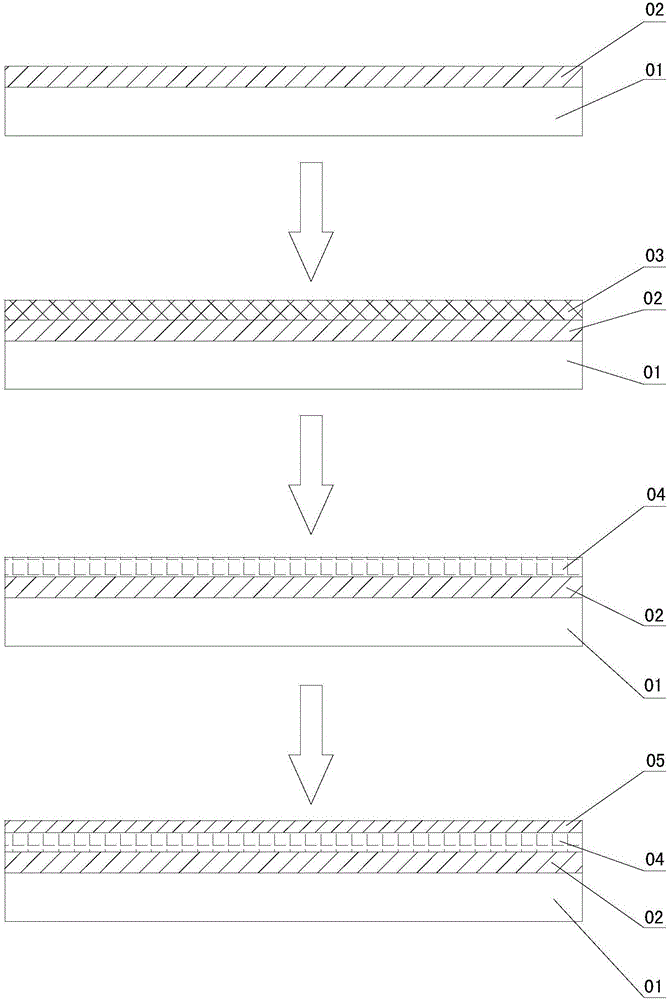
[0020] choose first figure 1 As shown in the substrate, the substrate includes a plate-shaped material 01 with a flat surface, and a layer of molybdenum film 02 deposited on the plate-shaped material. As a preferred method for manufacturing thin-film solar cells, the plate material 01 may be flat glass or a treated stainless steel plate or a treated polyimide plate. The substrate described above is an existing structure. After the substrate selection is completed, the following implementation steps are carried out:

[0021] 1. Sputter a layer of copper-gallium alloy thin film with a thickness of 0.2-2.5 μm on the substrate by vacuum sputtering. The specific method is to place the above-mentioned substrate in a vacuum sputtering chamber provided with a copper-gallium alloy target, and deposit a layer of copper-gallium alloy film by physical sputtering. The copper-gallium alloy film of the copper-gallium alloy film The two elements of gallium and copper come from the same cop...


PUM


Abstract

The invention discloses a method for preparing photoelectric absorption and conversion layers of copper, indium, gallium and selenium thin film solar cells.The method sequentially includes basic steps of 1), depositing each copper and gallium alloy thin film by the aid of processes for physically sputtering and depositing thin films under vacuum conditions; 2), carrying out selenation treatment on the copper and gallium alloy thin films in vacuum evaporation film coating selenium steam environments; 3), depositing indium and selenium elements on the thin films by the aid of vacuum co-evaporation processes after the thin films are subjected to selenation treatment; 4), depositing a small quantity of gallium on the thin films by the aid of vacuum evaporation processes to regulate electric properties of the photoelectric absorption and conversion layers of the copper, indium, gallium and selenium thin film solar cells.

Description

technical field [0001] The invention relates to a preparation method of a photoelectric absorption conversion layer of a solar cell. Background technique [0002] Copper indium gallium selenide thin-film solar cell is a kind of high-efficiency thin-film solar cell. The photoelectric absorption conversion layer of the solar cell is a compound semiconductor thin film composed of four elements: copper, indium, gallium and selenium. The photoelectric absorption conversion layer of the solar cell is currently prepared There are two methods of co-evaporation and selenization after sputtering. [0003] Co-evaporation method to prepare copper indium gallium selenide compound semiconductor film is as follows: four solid substances of copper, indium, gallium and selenium are respectively placed in their own independent evaporation sources, and the independent evaporation sources are heated separately so that they can be placed in them. Above the temperature at which the solid substan...

Claims


Application Information

Patent Timeline
Patent Type & Authority Applications(China)
IPC IPC(8): H01L31/032H01L31/18C23C14/24C23C14/34
CPCC23C14/24C23C14/34H01L31/0322H01L31/18Y02E10/541Y02P70/50
Inventor 陈良范孙嵩泉甄永泰
Owner ANHUI HERZE CIGS TECH CO LTD
Why Eureka
Try Eureka