Mono-crystalline silicon double-sided solar cell and preparation method thereof

A technology of double-sided solar cells and single crystal silicon, which is applied in the field of solar cells to achieve the effects of improving quantum conversion efficiency, optimizing surface recombination and optical absorption characteristics, and reducing surface area

Active Publication Date: 2016-08-03
TRINA SOLAR CO LTD
View PDF4 Cites 14 Cited by
  • Summary
  • Abstract
  • Description
  • Claims
  • Application Information

AI Technical Summary

Problems solved by technology

Although this densely distributed pyramid is beneficial to absorb direct light to the maximum, it is not necessarily the best light-absorbing structure for diffuse light, and the higher surface area will bring minority carrier recombination

Method used


Image

  • Mono-crystalline silicon double-sided solar cell and preparation method thereof
  • Mono-crystalline silicon double-sided solar cell and preparation method thereof

Examples


Embodiment 1

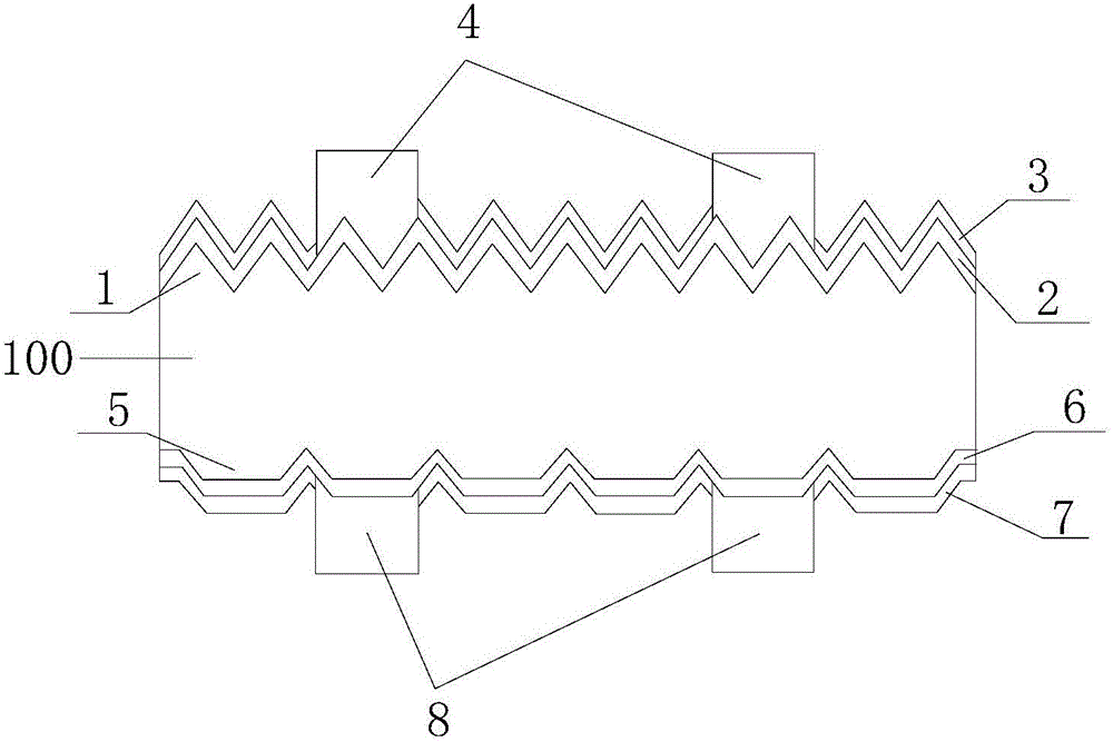
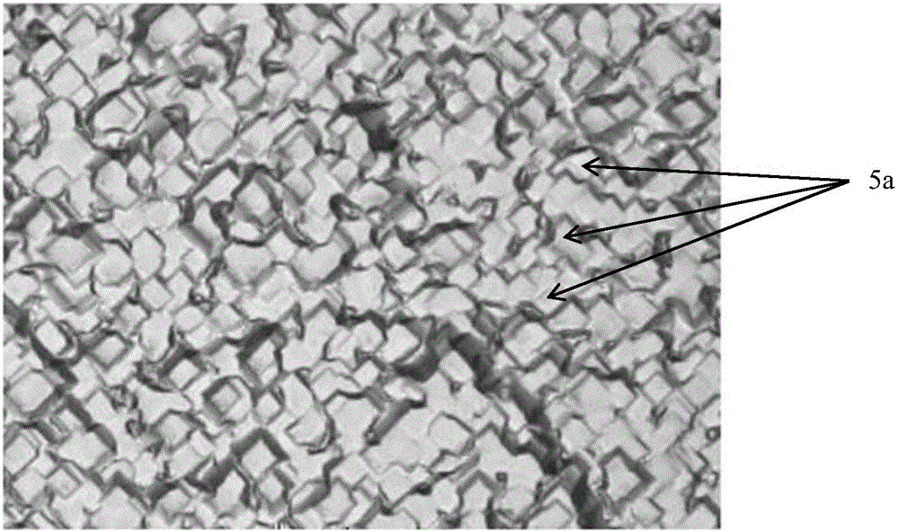
[0031] This embodiment is the case where the present invention is applied to P-type single crystal silicon. Such as figure 1 As shown, on the front side of the P-type single crystal silicon substrate 100, a front textured topographic structure 1 is sequentially formed, in this embodiment, it is a front pyramid-shaped textured surface, a front phosphorus-doped emitter junction 2, and a front passivation anti-reflection medium. layer 3 and the front electrode 4, on the back of the P-type single crystal silicon substrate, the back texturing topography structure 5, the boron-doped back surface field 6 formed by boron doping on the back, the back passivation anti-reflection dielectric layer 7 and back electrode 8, where, as figure 2 As shown, the back surface texture structure 5 is a platform-shaped suede surface, and each platform structure 5a is scattered, or partially connected, or partially overlapped, or distributed on the silicon substrate in a partially dispersed, partiall...

Embodiment 2

[0034] The difference between this embodiment and Embodiment 1 lies in that in the textured topography structure 5 on the back, each platform structure 5 a is distributed on the silicon substrate in a partially dispersed and partially connected manner. The side length of the plane on the platform structure 5 a is 10 μm, and the height of the platform structure 5 a is 8 μm. The front passivation anti-reflection medium layer 3 is a single-layer film made of silicon oxynitride with a film thickness of 70 to 80 nm; the back passivation anti-reflection medium layer 7 is a double-layer film made of titanium oxide and silicon oxide, wherein, The titanium oxide film has a thickness of 20 to 30 nm and the silicon oxide film has a thickness of 50 to 70 nm. Both the front electrode 4 and the back electrode 8 are copper electrodes.

Embodiment 3

[0036] This embodiment is a case where the present invention is applied to N-type single crystal silicon. Such as figure 1 As shown, on the front side of the N-type single crystal silicon substrate 100, a front pyramid-shaped textured surface 1, a front boron-doped emitter junction 2, a front passivation anti-reflection dielectric layer 3, and a front electrode 4 are sequentially formed. The back surface of the silicon substrate is sequentially formed with a back textured topographic structure 5, a phosphorus-doped back surface field 6 formed by phosphor doping on the back, a back passivation anti-reflection dielectric layer 7, and a back electrode 8, wherein the back textured topographic structure 5 is a platform-shaped suede surface, and each platform structure 5a is dispersedly distributed on the silicon substrate. Such as figure 1 As shown, the platform structure 5a has a lower plane connected to the silicon substrate 100 and an upper plane opposite to the lower plane. T...


PUM


Abstract

The invention discloses a mono-crystalline silicon double-sided solar cell. A front texturing morphology structure (1), a front PN emitter junction (2), a front passivated anti-reflection medium layer (3) and a front electrode (4) are sequentially formed on the front of a mono-crystalline silicon substrate (100). A back texturing morphology structure (5), a back surface field (6), a back passivated anti-reflection medium layer (7) and a back electrode (8) are sequentially formed on the back of the mono-crystalline silicon substrate. The solar cell is characterized in that the back texturing morphology structure (5) is a platform type texture surface, and platform structures (5a) are distributed on the mono-crystalline silicon substrate in a scattered, or tiled, or partially scattered, partially tiled, partially connected and partially overlapped way. The invention further discloses a preparation method of the mono-crystalline silicon double-sided solar cell. The minority carrier surface recombination and optical absorption characteristics of the double-sided solar cell are optimized, and the efficiency of quantum conversion is improved.

Description

technical field [0001] The invention relates to a solar cell and a preparation method thereof, in particular to a single crystal silicon double-sided solar cell and a preparation method thereof, belonging to the technical field of solar cells. Background technique [0002] The pursuit of improving battery conversion efficiency while reducing or even maintaining manufacturing costs is the goal that the industry is constantly pursuing and where it can improve its own competitiveness. Compared with traditional crystalline silicon solar cells that receive light on one side, double-sided solar cells use two light-receiving surfaces, the front and the back, to obtain higher photocurrent densities and greatly increase power generation. Depending on the installation ground and environment, a photovoltaic power generation system based on bifacial solar cells can achieve a power gain of 10 to 30%. [0003] The structure of double-sided solar cells includes: front and back textured su...

Claims


Application Information

Patent Timeline
Patent Type & Authority Applications(China)
IPC IPC(8): H01L31/0236H01L31/18
CPCH01L31/02366H01L31/1804Y02E10/547Y02P70/50
Inventor 盛赟陈奕峰崔艳峰袁声召端伟元王子港
Owner TRINA SOLAR CO LTD
Why Eureka
Try Eureka