Photoelectrochemical etching method for removing SiC substrate epitaxial graphene buffer layer

A photoelectrochemical and graphene technology, applied in the field of microelectronic materials, can solve the problems of strong corrosiveness, high risk factor, severe hydrofluoric acid-metal molybdenum reaction process, etc., to achieve high safety factor, safe operation, fixed assets, etc. less investment

Inactive Publication Date: 2016-08-10
SHANDONG UNIV
View PDF4 Cites 4 Cited by
  • Summary
  • Abstract
  • Description
  • Claims
  • Application Information

AI Technical Summary

Problems solved by technology

However, in the process described in the above-mentioned patent documents, the hydrofluoric acid-metal molybdenum reaction process is violent a

Method used


Image

  • Photoelectrochemical etching method for removing SiC substrate epitaxial graphene buffer layer
  • Photoelectrochemical etching method for removing SiC substrate epitaxial graphene buffer layer
  • Photoelectrochemical etching method for removing SiC substrate epitaxial graphene buffer layer

Examples


Embodiment 1

[0038] A photoelectrochemical etching method for removing an epitaxial graphene buffer layer on a SiC substrate, comprising steps as follows:

[0039] (1) Polish and clean the 6H-SiC wafer with a diameter of 2 inches after silicon surface polishing, and complete the growth of graphene in a single crystal growth furnace to obtain a 4H / 6H‐SiC substrate epitaxial graphene wafer; the growth temperature is 1650 ℃, the growth time is 60min;

[0040] Heat the electric soldering iron to 120°C and place it on the indium grain to melt the metal indium; place one end of a 15cm-long metal nickel wire in the molten metal indium and let it stand for 0.5min to fix the metal wire on the metal indium grain , as a wire connecting the epitaxial graphene wafer on the 4H / 6H-SiC substrate;

[0041] Weigh 1.000g KOH solid, dissolve in 50mL deionized water, stir evenly with a glass rod, let stand for 4min, and prepare 2wt% KOH etching solution;

[0042] The obtained 4H / 6H-SiC substrate epitaxial gr...

Embodiment 2

[0048] A photoelectrochemical etching method for removing an epitaxial graphene buffer layer on a SiC substrate, comprising steps as follows:

[0049] According to the same graphene growth method as in Example 1, the difference is that a certain amount of KOH is weighed, fully stirred and dissolved in 50 mL of deionized water, and a 3wt% KOH etching solution is prepared.

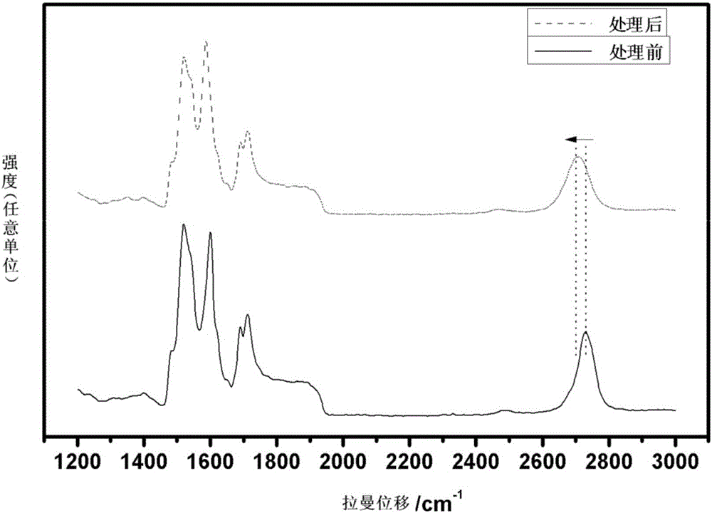
[0050] Graphene material obtained by Raman spectrum and AFM characterization, the 2D peak position is 2672cm -1 , width at half peak is 65.1cm -1 .

Embodiment 3

[0052] A photoelectrochemical etching method for removing an epitaxial graphene buffer layer on a SiC substrate, comprising steps as follows:

[0053] According to the same graphene growth method as in Example 1, the difference is that the three-electrode system is irradiated with ultraviolet light, and the electrolysis time is controlled for 2 hours.

[0054] Graphene material obtained by Raman spectrum and AFM characterization, the 2D peak position is 2682cm ‐1 , width at half peak is 58.3cm ‐1 .

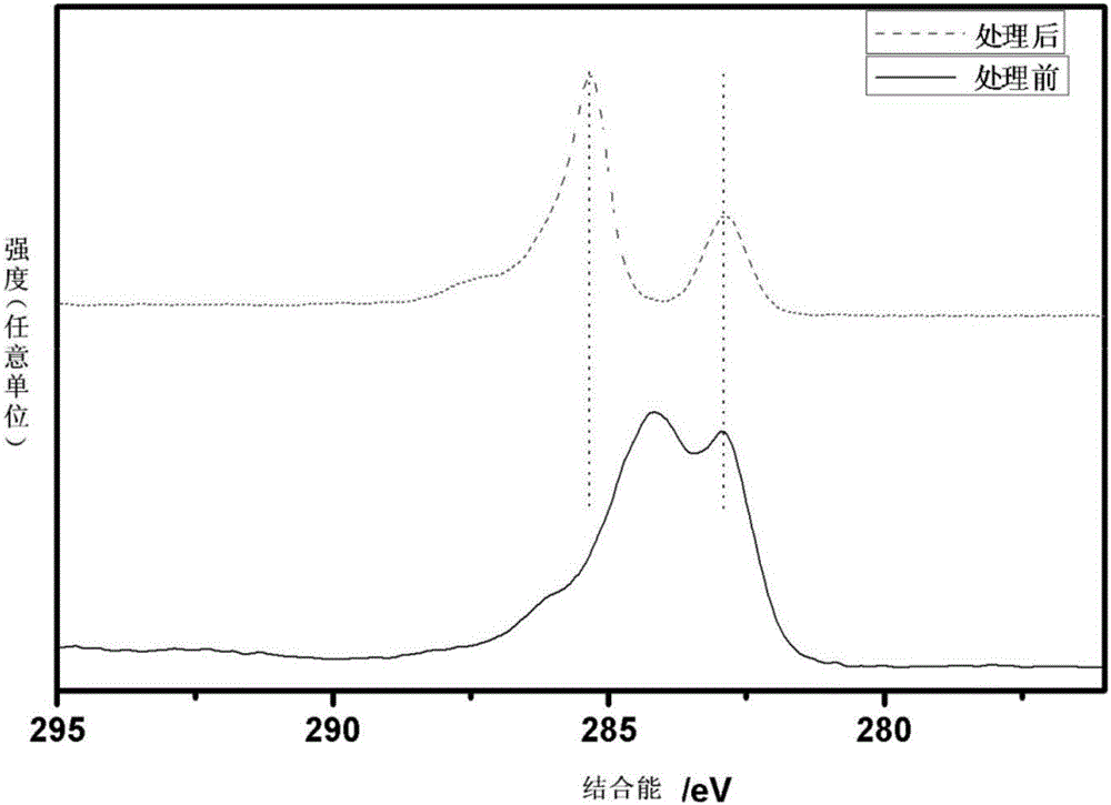
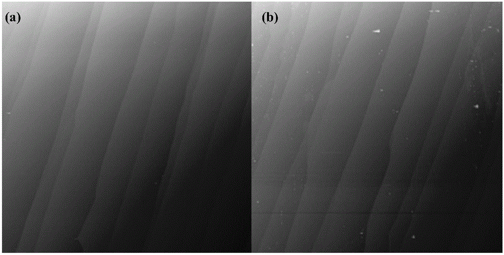
[0055] Through the description of Examples 1-3, in conjunction with the characterization results of graphene materials under the three embodiments, it can be seen that the application of the method of the present invention can eliminate the friction between graphene and the underlying SiC substrate without destroying the surface graphene. Interaction and uniform surface morphology are conducive to improving the performance of graphene materials in the field of electrical devices...


PUM


Abstract

The invention relates to a photoelectrochemical etching method for removing an epitaxial graphene buffer layer on a SiC substrate, comprising the following steps: (1) connecting a SiC substrate epitaxial graphene wafer to metal indium as a working electrode; using a saturated calomel electrode or The silver/silver chloride electrode is used as the reference electrode, the platinum electrode is used as the counter electrode, and the KOH solution is used as the etching solution; the working electrode, the reference electrode and the counter electrode are placed in the etching solution, and a three-electrode system is assembled; (2 ) Irradiate the three-electrode system with ultraviolet light, and control the electrolytic current density to 1.0-2.0mA/cm 2 , the buffer layer can be removed by photoelectrochemical etching on the SiC substrate epitaxial graphene buffer wafer. By optimizing the process parameters in the method of the invention, the buffer layer can be completely removed, and a graphene material with a uniform surface can be obtained.

Description

technical field [0001] The invention relates to a processing method for removing an epitaxial graphene buffer layer on a SiC substrate, in particular to a photoelectrochemical etching method based on a large-diameter 4H / 6H-SiC substrate epitaxially growing graphene, and belongs to the technical field of microelectronic materials. Background technique [0002] Graphene is made of carbon atoms with sp 2 The atomic-level two-dimensional crystal material of the hexagonal honeycomb lattice formed by orbital hybridization has a high carrier mobility dozens of times that of commercial silicon wafers, and is little affected by temperature and doping effects, showing excellent Electron transport properties. Graphene crystals have important application value in ultra-high frequency electronic devices. However, the improvement of the performance of graphene electronic devices is severely restricted by the quality of graphene, and the preparation of high-quality, low-cost graphene mat...

Claims


Application Information

Patent Timeline
IPC IPC(8): H01L21/02
CPCH01L21/02019
Inventor 陈秀芳孙丽徐现刚赵显
Owner SHANDONG UNIV
Why Eureka
Try Eureka