A scale-up method for CVD-grown large-area graphene

A graphene, large-area technology, applied in the field of high-efficiency CVD growth of large-area graphene, can solve problems such as uneven growth of graphene, and achieve the effects of increasing the loading capacity of a single batch, increasing the output, and reducing the cost of raw materials

Active Publication Date: 2018-01-16
INST OF METAL RESEARCH - CHINESE ACAD OF SCI +1
View PDF2 Cites 0 Cited by
  • Summary
  • Abstract
  • Description
  • Claims
  • Application Information

AI Technical Summary

Problems solved by technology

[0004] In view of the above-mentioned problems existing in the existing CVD preparation methods, the purpose of the present invention is to provide a low-cost, high-efficiency CVD large-scale method for growing large-area graphene. The yield of large-area graphene grown in batches, while solving the problem of uneven graphene growth in the prior art when the loading capacity is high

Method used


Image

  • A scale-up method for CVD-grown large-area graphene

Examples


Embodiment 1

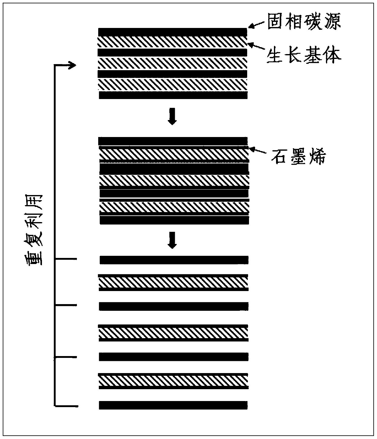
[0028] Such as figure 1 As shown, metal copper foil (25 μm thick) was used as the growth substrate, and carbon felt (50 μm thick) was used as the solid-phase carbon source. The flat large-area copper foil and carbon felt are stacked alternately, and the number of layers is 200 layers. Put the laminated copper foil and carbon felt into an electrically heated CVD furnace for growth. First, vacuumize the furnace chamber until the pressure is less than 1Pa, then feed in hydrogen gas with a flow rate of 100 sccm, and maintain the pressure at 50Pa; within 30 minutes, raise the furnace temperature to 1000°C, keep it for 10 minutes and then cool it down to room temperature with the furnace. Complete CVD growth. High-quality large-area single-layer graphene is formed on both the upper and lower surfaces of the copper foil, while the carbon felt can be reused for CVD growth.

Embodiment 2

[0030] The difference with Example 1 is:

[0031] Other materials are used as solid-phase carbon sources, including flexible graphite paper, carbon nanotube film, fullerene, carbon black or silicon carbide, etc.; the growth is carried out by atmospheric pressure CVD process, and the carrier gas is argon.

Embodiment 3

[0033] Such as figure 1 As shown, a quartz plate coated with a nickel film (500 nm thick) was used as the growth substrate, and a carbon fiber cloth (200 μm thick) impregnated with epoxy resin was used as the solid-phase carbon source. The nickel film / quartz plate and the carbon fiber / resin cloth are stacked alternately, and the number of layers is 100. The stacked samples were placed in an induction heating CVD furnace for growth. First vacuumize the furnace cavity until the pressure is less than 1Pa, then introduce hydrogen with a flow rate of 50sccm, and maintain the pressure at 20Pa; within 3 minutes, raise the furnace temperature to 1000°C and keep it for 1 minute; then stack the samples Perform rapid cooling to room temperature at a cooling rate of 15° C. / second to complete CVD growth. High-quality large-area few-layer graphene is formed on the surface of the nickel film, and the carbon fiber cloth can be reused for CVD growth.

[0034] The results of the examples sho...


PUM

PropertyMeasurementUnit
electron mobilityaaaaaaaaaa

Abstract

The invention relates to a graphene preparation technology, in particular to a large-scale method for growing large-area graphene by CVD. The method improves the yield of large-area graphene grown in a single batch by adopting a method of alternately stacking growth substrates and solid-phase carbon sources in CVD growth. The invention uses a planar growth substrate and a recyclable solid-phase carbon source, alternately stacks the two for CVD growth, forms large-area graphene on the upper and lower surfaces of the growth substrate, and reuses the solid-phase carbon source. The method of alternately stacking the growth substrate and the solid-phase carbon source greatly increases the single-batch loading capacity of the growth substrate, and realizes the growth of high-quality large-area graphene on both the upper and lower surfaces of the growth substrate, thereby increasing the growth rate of graphite in a single batch. ene production. The use of recyclable solid-phase carbon sources can avoid the high production cost caused by the large consumption of high-purity gas-phase carbon sources, so it can be used as a low-cost, high-efficiency large-scale method for producing large-area graphene.

Description

Technical field: [0001] The invention relates to a graphene preparation technology, specifically a large-scale method for growing large-area graphene by high-efficiency CVD in a manner of alternately stacking growth substrates and solid-phase carbon sources. Background technique: [0002] Graphene is a two-dimensional honeycomb crystal structure formed by densely packing a single layer of carbon atoms, and is the basic structural unit for constructing other dimensional carbon materials (zero-dimensional fullerene, one-dimensional carbon nanotubes, and three-dimensional graphite). The unique crystal structure of graphene makes it have excellent electrical, thermal and mechanical properties, such as: its electron mobility is as high as 200,000 cm at room temperature 2 / V s, the thermal conductivity is as high as 5300W / m k, and it is expected to be obtained in the fields of multifunctional nanoelectronic devices, transparent conductive films, composite materials, catalytic mate...

Claims


Application Information

Patent Timeline
Patent Type & Authority Patents(China)
IPC IPC(8): C01B32/188
Inventor 任文才马来鹏成会明
Owner INST OF METAL RESEARCH - CHINESE ACAD OF SCI
Why Eureka
Try Eureka