Surface enhanced Raman spectrum substrate with nano gap and preparation method thereof

A nano-gap and substrate technology, applied in Raman scattering, nanotechnology, nanotechnology, etc., can solve the problems of cumbersome steps and cumbersome and complicated preparation methods, and achieve the effect of improving sensitivity

Active Publication Date: 2016-08-31
TECHNICAL INST OF PHYSICS & CHEMISTRY - CHINESE ACAD OF SCI
View PDF5 Cites 10 Cited by
  • Summary
  • Abstract
  • Description
  • Claims
  • Application Information

AI Technical Summary

Problems solved by technology

However, these methods are subject to certain limitations. The photolithography method is limited by the diffraction limit, and the gap that can be prepared can only reach about 10nm. The template method and the method of etching the sacrificial layer are cumbersome, and the preparation method is cumbersome and complicated.
Currently, there is still a lack of a quick and easy method for preparing SERS substrates with nanogap

Method used


Image

  • Surface enhanced Raman spectrum substrate with nano gap and preparation method thereof
  • Surface enhanced Raman spectrum substrate with nano gap and preparation method thereof
  • Surface enhanced Raman spectrum substrate with nano gap and preparation method thereof

Examples


Embodiment 1

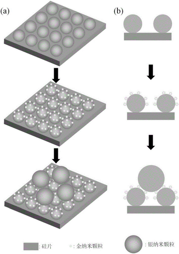
[0042] Example 1: Preparation of a SERS substrate with nano-gap

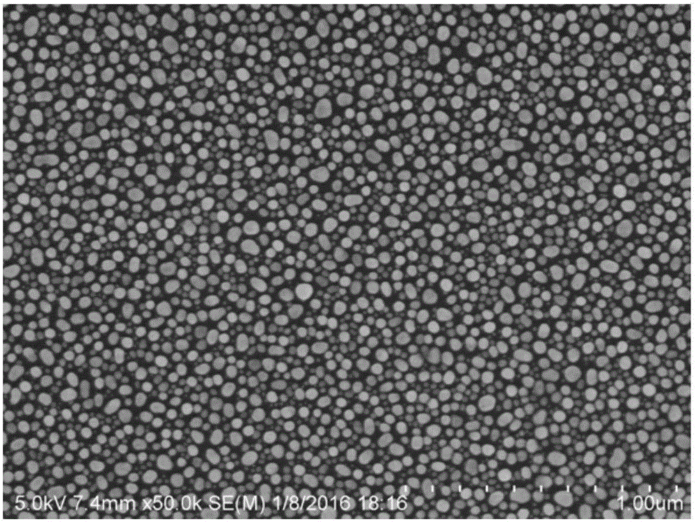
[0043]Preparation of the first layer of silver nanoparticles: Ultrasonic cleaning was performed on the monocrystalline silicon wafer using acetone, ethanol, and distilled water in sequence, and the ultrasonic cleaning time was 10 minutes each time. Soak the cleaned silicon chip in a mixed solution of silver nitrate and hydrofluoric acid for 10 seconds, wherein the concentration of silver nitrate in the mixed solution is 5 mmol / L, and the concentration of hydrofluoric acid is 4.8 mol / L. Among them, the silver nanoparticles on the silicon chip obtained are heated up from room temperature (about 20° C.) to 160° C. in a pure argon atmosphere for 30 minutes, and after being kept for 20 minutes, the temperature is naturally cooled to room temperature to obtain the silver nanoparticles attached to the single crystal silicon. The first layer of silver nanoparticles on the chip, the SEM picture is as follows figure 2 A...

Embodiment 2

[0051] Embodiment 2: Raman spectrum signal test of SERS substrate

[0052] The Raman spectrum signal intensity of the SERS substrate prepared in Comparative Example 1 and Comparative Example 1 was compared. The specific test method is as follows:

[0053] 4-Mercaptopyridine molecules are dissolved in ethanol, and the concentration of 4-Mercaptopyridine molecules is 1mmol / L. The substrate was immersed in the ethanol solution for 1 hour, and after being taken out, it was rinsed with ethanol, dried with nitrogen, and then detected by Raman spectroscopy. 4-mercaptopyridine can form a 4-mercaptopyridine monomolecular layer on the silver surface through a chemical reaction between the mercapto group and the silver atom on the substrate. The obtained SERS spectrum is as Figure 6 As shown, the experimental results show that: in the detection of 4-mercaptopyridine molecules at the same molar concentration, the SERS substrate of Example 1 showed a stronger Raman spectrum signal inte...

Embodiment 3

[0054] Example 3: Preparation of a SERS substrate with nano-gap

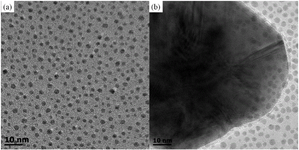
[0055] The method for preparing the first layer of silver nanoparticles is the same as in Example 1. The method for depositing gold nanoparticles is the same as in Example 1, wherein the sputtering time is 3s, and the TEM pictures of the sputtered gold nanoparticles and the sputtered gold nanoparticles to the first layer of silver nanoparticles are as follows Figure 7 a and Figure 7 As shown in b, the average diameter of the obtained gold nanoparticles is 2 nm. The method of preparing the silver nanoparticle dispersion solution is the same as in Example 1. The method of spin-coating the second layer of silver nanoparticles is the same as in Example 1.


PUM

PropertyMeasurementUnit
diameteraaaaaaaaaa
diameteraaaaaaaaaa
diameteraaaaaaaaaa

Abstract

The invention discloses a surface enhanced Raman spectrum substrate with a nano gap and a preparation method thereof. The surface enhanced Raman spectrum substrate with the nanometer gap is composed of first-layer silver nanoparticles attached on a monocrystal silicon slice and having the surface loaded with gold nanoparticles and second-layer silver nanoparticles spin-coated on the first-layer silver nanoparticles. By depositing a certain size and distribution of gold nanoparticles, the nano gap is formed between the two layers of silver nanoparticles. The surface enhanced Raman spectrum substrate with the nano gap is used for detecting 4-pyridinethiol molecules in an ethanol solution, the obtained Raman spectrum signal intensity is two times that of a substrate without gold nanoparticles. The invention provides a means for preparing the nano gap to enhance the surface enhanced Raman spectrum signal, and the reference significance is provided for preparation of the high-performance surface enhanced Raman spectrum substrate.

Description

technical field [0001] The invention belongs to the field of Raman spectrum substrates, and relates to a surface-enhanced Raman spectrum substrate with nano-gap and a preparation method thereof. Background technique [0002] Surface-enhanced Raman scattering (SERS) technology has the characteristics of high sensitivity, high resolution, selective recognition, quenchable fluorescence, and good stability, and has high potential application value in the fields of surface science, spectroscopy, and biochemical detection. . [0003] The basis for the application of SERS technology is the development of active substrates with high sensitivity. The key to obtaining a highly sensitive SERS substrate is to form a large number of SERS "hot spots" on the substrate, and the local electromagnetic field at the "hot spots" is greatly enhanced, thereby improving the sensitivity of the SERS substrate. Fabrication of nanogap on SERS substrate can generate SERS "hot spot" and enhance SERS si...

Claims


Application Information

Patent Timeline
Patent Type & Authority Applications(China)
IPC IPC(8): G01N21/65B82Y30/00B82Y40/00
CPCB82Y30/00B82Y40/00G01N21/658
Inventor 佘广为金亮亮师文生
Owner TECHNICAL INST OF PHYSICS & CHEMISTRY - CHINESE ACAD OF SCI
Why Eureka
Try Eureka