
Preparation method for micro-piezoelectric actuator array structure

An array structure and driver technology, applied in the manufacture/assembly of piezoelectric/electrostrictive devices, piezoelectric/electrostrictive/magnetostrictive devices, circuits, etc., can solve the complex preparation method, compactness and piezoelectricity Poor performance and other problems, to achieve the effect of simple and easy process flow, guaranteed compactness and piezoelectric performance, suitable for batch preparation

Inactive Publication Date: 2016-09-21
SHANGHAI INST OF TECH
View PDF3 Cites 4 Cited by
  • Summary
  • Abstract
  • Description
  • Claims
  • Application Information

AI Technical Summary

Problems solved by technology

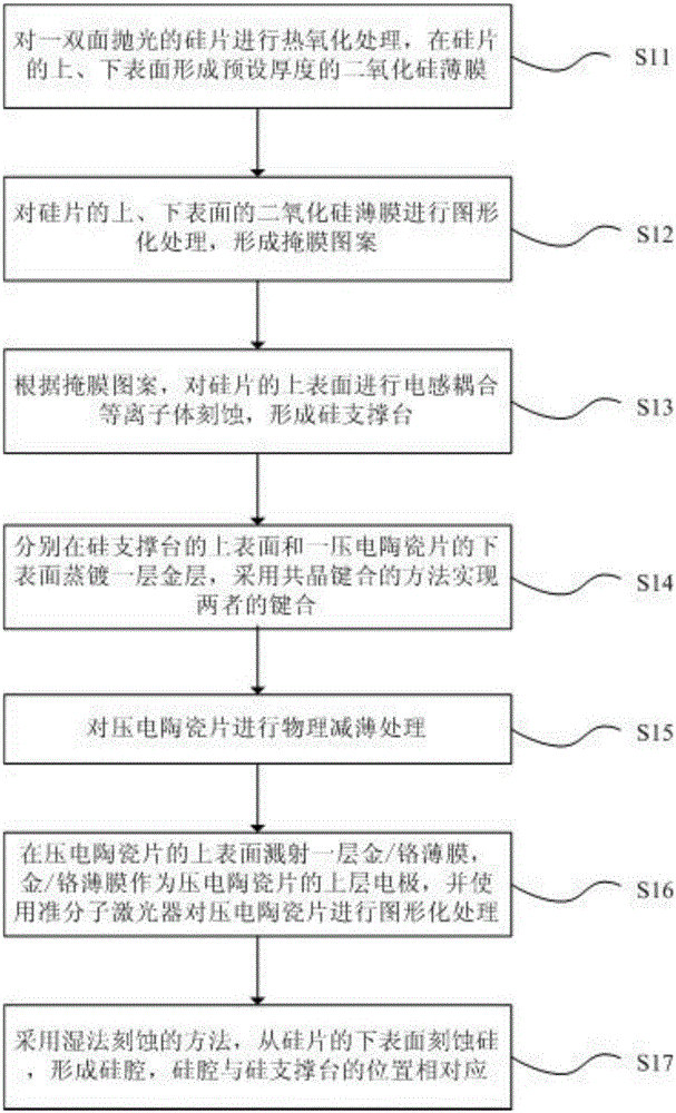
[0004] In view of the problems existing in the above-mentioned prior art, the present invention proposes a method for preparing a micro-piezoelectric driver array structure, and adopts the physical thinning method of bulk piezoelectric ceramics to realize the preparation of piezoelectric thick films. The performance can be greatly guaranteed; and the combination of the inductively coupled plasma etching and the wet etching process, the method steps are simple and easy, and solve the problems of complex preparation methods, poor compactness and poor piezoelectric performance in the prior art. question

Method used


Image

  • Preparation method for micro-piezoelectric actuator array structure
  • Preparation method for micro-piezoelectric actuator array structure
  • Preparation method for micro-piezoelectric actuator array structure

Examples


Embodiment Construction

[0037] The embodiments of the present invention are described in detail below. This embodiment is implemented on the premise of the technical solution of the present invention, and detailed implementation methods and specific operating procedures are provided, but the protection scope of the present invention is not limited to the following implementation example.

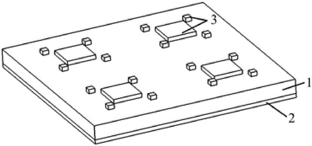
[0038] combine Figure 1-Figure 7 , the preparation method of the micro piezoelectric actuator array structure of the present invention is described in detail, and its flow chart is as follows figure 1 As shown, it includes the following steps:

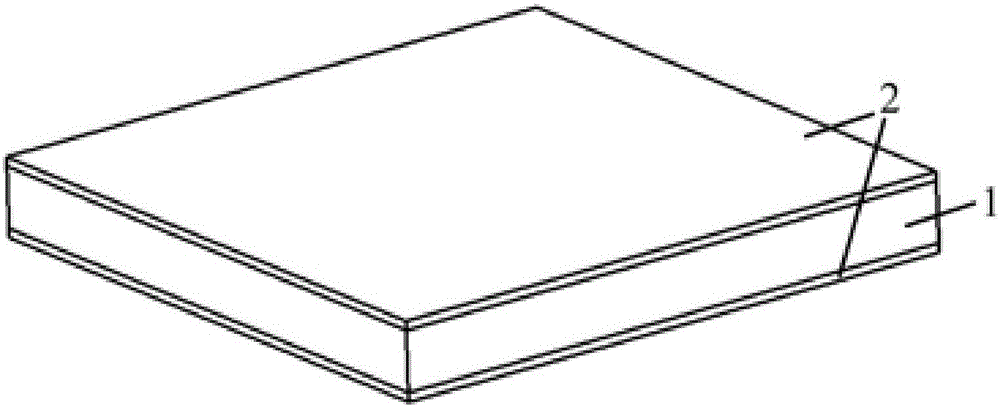
[0039] S11: Take a 20mm*20mm, 300um thick double-sided polished silicon wafer 1, wash and dry it, put it into a thermal oxidation furnace for thermal oxidation treatment, so that the upper and lower surfaces of the silicon wafer are formed A silicon dioxide film 2 with a preset thickness, the schematic diagram of the silicon wafer structure after this step is as follows ...


PUM


Abstract

The invention discloses a preparation method for a micro-piezoelectric actuator array structure. The preparation method comprises the steps of carrying out thermal oxidation treatment on a silicon wafer, wherein the two sides of the silicon wafer are polished, and forming a silicon dioxide thin film on the surface; carrying out patterning treatment on the silicon dioxide thin film to form a mask pattern; carrying out inductive coupling plasma etching on the upper surface of the silicon wafer according the mask pattern to form a silicon supporting table; evaporating a gold layer on the upper surface of the silicon supporting table and the lower surface of a piezoelectric ceramic sheet separately, and bonding the silicon supporting table and the piezoelectric ceramic sheet by adopting an eutectic bonding method; carrying out physical thinning on the piezoelectric ceramic sheet; sputtering a gold / chromium thin film on the upper surface of the piezoelectric ceramic sheet to be used as the upper layer electrode of the piezoelectric ceramic sheet, and carrying out patterning treatment on the piezoelectric ceramic sheet by an excimer laser; and etching silicon from the lower surface of the silicon wafer by a wet etching method to form a silicon cavity, wherein the position of the silicon cavity is corresponding to that of the silicon supporting table. The micro-piezoelectric actuator array structure is simple and easy to implement the preparation method and high in compactness and piezoelectric property.

Description

technical field [0001] The invention relates to the field of micro-electromechanical technology, in particular to a method for preparing a piezoelectric driver array structure. Background technique [0002] In recent years, microreactors, microfluidic analysis chips, etc. have been actively promoting the research of medical microfluidic systems. Among them, the microfluidic analysis chip is a miniature total analysis system (μ-TAS) that integrates analysis functions such as sampling, dilution, reagent addition, reaction, separation, and detection to the greatest extent. , life sciences, chemical synthesis, analytical instruments and environmental sciences and many other important frontiers of development. The PZT film used for micro-piezoelectric drive is the main part of the micro-driver in the micro-fluidic analysis chip, and is the power source for driving the sample in the micro-fluidic analysis chip. [0003] At present, the preparation methods of PZT thin films for m...

Claims


Application Information

Patent Timeline
Patent Type & Authority Applications(China)
IPC IPC(8): H01L41/22H01L41/337H10N30/01H10N30/086
CPCH10N30/01H10N30/086
Inventor 李以贵黄远颜平王欢胡隆胜夏碧颖李俊衡桑先润
Owner SHANGHAI INST OF TECH
Learn More