Beam lead capacitor processing method

A beam-type lead wire and processing method technology, which is applied to fixed capacitor parts, fixed capacitor electrodes, fixed capacitor dielectrics, etc., can solve the problems of complex processing, difficult silicon etching, and high production costs, and achieve reduction in process flow, The effect of improving processing efficiency and reducing the difficulty of substrate etching

Active Publication Date: 2016-10-12
THE 41ST INST OF CHINA ELECTRONICS TECH GRP
View PDF6 Cites 4 Cited by
  • Summary
  • Abstract
  • Description
  • Claims
  • Application Information

AI Technical Summary

Problems solved by technology

The beam-type lead capacitors produced by AEROFLEX in the United States are manufactured using silicon-based semiconductor technology. Because silicon etching is very difficult, a large investment in semiconductor process equipment is required. The processing process is complicated, resulting in high production costs.

Method used


Image

  • Beam lead capacitor processing method
  • Beam lead capacitor processing method
  • Beam lead capacitor processing method

Examples


Embodiment 1

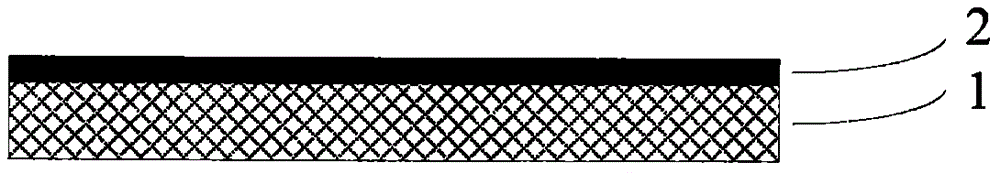
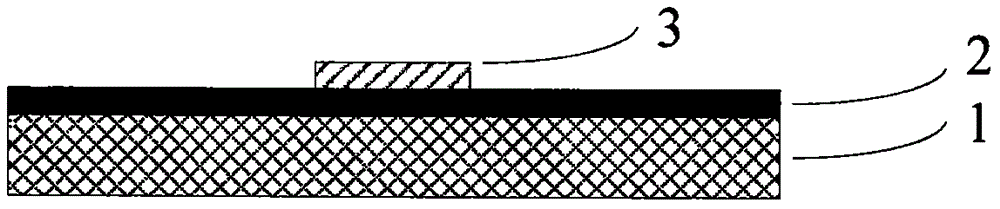
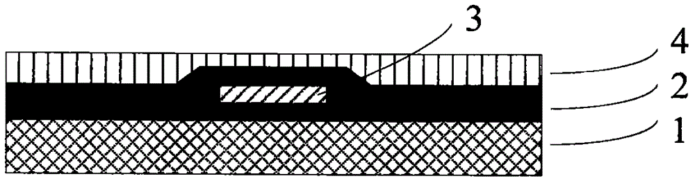
[0030] A method for processing a beam-type lead capacitor provided by the present invention mainly includes: the first step, selecting a nickel plate 1 with a thickness of 0.1 mm as a mechanical support, and forming a layer of TiW metal film 2 on the nickel plate by sputtering coating method , the schematic diagram of the structure is as figure 1 As shown; in the second step, the polyimide dielectric film is covered 3 to cover the entire nickel plate 1 by spin coating, and then the required graphics are retained by photolithography. The schematic diagram of the structure is as follows figure 2 As shown; in the third step, a layer of TiW / Au metal layer structure is formed by sputtering coating method, covering the existing polyimide dielectric film 3, and the metal layer structure formed on the nickel plate is TiW-Au, and the structural diagram is as follows image 3 As shown, wherein the mass ratio of titanium to tungsten is 1:9; the fourth step is to apply glue on the substr...

Embodiment 2

[0032] The processing method of a beam-type lead capacitor provided by the present invention mainly includes: the first step, select a nickel plate 1 with a thickness of 0.5 mm as a mechanical support, and form a layer of TiW metal film 2 on the nickel plate by sputtering coating method , the schematic diagram of the structure is as figure 1 As shown; in the second step, the polyimide dielectric film is covered 3 to cover the entire nickel plate 1 by spin coating, and then the required graphics are retained by photolithography. The schematic diagram of the structure is as follows figure 2 As shown; in the third step, a layer of TiW / Au metal layer structure is formed by sputtering coating method, covering the existing polyimide dielectric film 3, and the metal layer structure formed on the nickel plate is TiW-Au, and the structural diagram is as follows image 3 As shown, wherein the mass ratio of titanium to tungsten is 1:9; the fourth step is to apply glue on the substrate, ...

Embodiment 3

[0034] The processing method of a kind of beam-type lead capacitor provided by the present invention mainly comprises: the first step, selects the nickel plate 1 of 1mm thickness as mechanical support, and adopts the sputter coating method to form a layer of TiW metal film 2 on the nickel plate, Structural diagram such as figure 1 As shown; in the second step, the polyimide dielectric film is covered 3 to cover the entire nickel plate 1 by spin coating, and then the required graphics are retained by photolithography. The schematic diagram of the structure is as follows figure 2 As shown; in the third step, a layer of TiW / Au metal layer structure is formed by sputtering coating method, covering the existing polyimide dielectric film 3, and the metal layer structure formed on the nickel plate is TiW-Au, and the structural diagram is as follows image 3 As shown, wherein the mass ratio of titanium to tungsten is 1:9; the fourth step is to apply glue on the substrate, pre-baking,...


PUM

PropertyMeasurementUnit
thicknessaaaaaaaaaa
thicknessaaaaaaaaaa

Abstract

The invention relates to a beam lead capacitor processing method, and the method comprises the following steps: 1, providing a nickel plate, and forming a TiW metal film on the nickel plate through employing a sputter coating method; 2, forming a polyimide dielectric film on the nickel plate through employing a photoetching method; 3, forming a TiW/Au metal layer structure through employing the sputter coating method, and covering the polyimide dielectric film; 4, forming the upper and lower electrodes of a beam lead capacitor through employing a photoetching electroplating method; 5, selectively etching the nickel plate through employing the photoetching method, maintaining the mechanical supporting action of the nickel plate, and enabling the upper and lower electrodes to form circuit break. The invention aims at providing the method which is simpler in processing. Compared with a method provided by a foreign manufacturer, the method improves the production efficiency, reduces the cost, and is worthy of polularization in production.

Description

technical field [0001] The invention relates to the technical field of semiconductors, in particular to a processing method of a beam-type lead capacitor. Background technique [0002] The main structure of the beam-type lead capacitor used in microwave module assembly is as follows: on a base material that provides mechanical support, the lower electrode, dielectric and upper electrode are respectively generated. Usually, the upper and lower electrodes are made of precious metal gold, and the dielectric Materials are selected according to different needs. At the same time, in order to facilitate assembly, the upper and lower electrodes are led out to the left and right sides, which is convenient for subsequent operations such as bonding and interconnection. [0003] The AEROFLEX company of the United States has produced a large number of beam-type lead capacitor products and occupied most of the global market. The beam-type lead capacitor produced by AEROFLEX in the Unite...

Claims


Application Information

Patent Timeline
Patent Type & Authority Applications(China)
IPC IPC(8): H01G4/002H01G4/005H01G4/14
CPCH01G4/002H01G4/005H01G4/14
Inventor 马子腾许延峰王进
Owner THE 41ST INST OF CHINA ELECTRONICS TECH GRP
Why Eureka
Try Eureka