Fin type fast recovery super-junction power semiconductor transistor and preparation method thereof

A technology of power semiconductors and transistors, applied in semiconductor/solid-state device manufacturing, semiconductor devices, final product manufacturing, etc., can solve the problems of increased device manufacturing cost, long time, high hardness of body diode reverse recovery, etc. The effect of the hole current path

Active Publication Date: 2016-10-12
SOUTHEAST UNIV
View PDF6 Cites 3 Cited by
  • Summary
  • Abstract
  • Description
  • Claims
  • Application Information

AI Technical Summary

Problems solved by technology

However, compared with the traditional MOSFET, the super junction structure has a significant disadvantage: the body diode reverse recovery hardness is high and the time is long
Traditional methods use electron irradiation or heavy metal doping to control the minority carrier lifetime, reduce the reverse recovery charge, and reduce the reverse recovery peak current, but this will increase the manufacturing cost of the device and lead to large leakage and reduced long-term reliability.

Method used


Image

  • Fin type fast recovery super-junction power semiconductor transistor and preparation method thereof
  • Fin type fast recovery super-junction power semiconductor transistor and preparation method thereof
  • Fin type fast recovery super-junction power semiconductor transistor and preparation method thereof

Examples


Embodiment 1

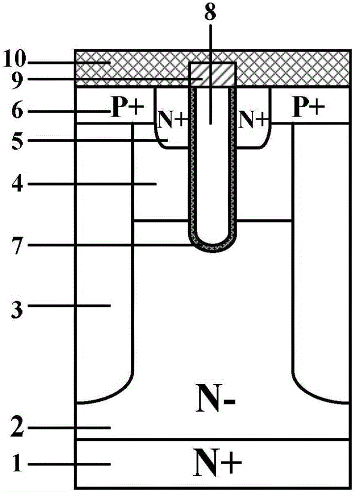
[0032] Combine below figure 2, the present invention is described in detail, a fin-type fast recovery super junction power semiconductor transistor, comprising: an N-type substrate 1, an N-type epitaxial layer 2 is arranged on the N-type substrate 1, and an inner layer of the N-type epitaxial layer 2 A columnar second P-type body region 3 is provided, and a first P-type body region 4 is provided on the top of the N-type epitaxial layer 2, and the first P-type body region 4 is located between two columnar second P-type body regions 3 An N-type heavily doped source region 5 and a P-type heavily doped semiconductor contact region 6 are provided on the surface of the first P-type body region 4, and an N-type heavily doped source region 5 and a P-type heavily doped semiconductor contact region 6 and the second P-type body region 3 are connected with a source metal 10, which is characterized in that polysilicon gates 8 are respectively arranged on both sides of the first P-type bod...

Embodiment 2

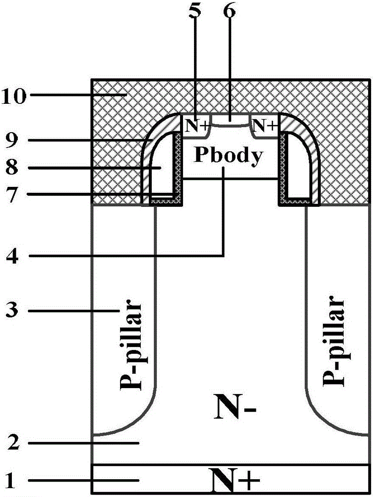
[0034] Combine below Figure 10 ~ Figure 18 , the present invention is described in detail, a method for preparing a fin-type fast recovery super-junction power semiconductor transistor, characterized in that:

[0035] The first step: first select N-type silicon material as the substrate and epitaxially grow N-type epitaxial layer;

[0036] Step 2: First, use a mask to selectively etch deep trenches in the N-type epitaxial layer, and epitaxially grow to form the second P-type body region 3;

[0037] Step 3: selectively etching the N-type epitaxial layer to form a convex epitaxial layer 2;

[0038] Step 4: Thermally grow a gate oxide layer 7 on the surface of the convex epitaxial layer 2, and then deposit polysilicon to fill the concave part of the N-type epitaxial layer 2;

[0039] Step 5: Etching the polysilicon to the surface of the raised portion of the N-type epitaxial layer 2, implanting boron ions, and annealing to form the first P-type body region 4;

[0040] Step 6:...


PUM


Abstract

The invention discloses a fin type fast recovery super-junction power semiconductor transistor and a preparation method thereof. The fin type fast recovery super-junction power semiconductor transistor comprises an N-type substrate, wherein an N-type epitaxial layer is arranged on the N-type substrate; second columnar P-type body regions are arranged in the N-type epitaxial layer; a first P-type body region is arranged on the top of the N-type epitaxial layer, and the first P-type body region is positioned between the two second columnar P-type body regions; the surface of the N-type epitaxial layer is provided with an N-type heavily-doped source region and a P-type heavily-doped semiconductor contact region; the N-type heavily-doped source region, the P-type heavily-doped semiconductor contact region and the second P-type body region are connected with source electrode metals; polysilicon gates are arranged on two sides of the first P-type body region respectively; the second columnar P-type body regions are terminated at the lower surfaces of the polysilicon gates, and the second columnar P-type body regions are lower than the first P-type body region; gate oxide layers are arranged between the polysilicon gates and the first P-type body region, the N-type epitaxial layer and the second P-type body regions; insulated layers are arranged between the polysilicon gates and the source electrode metals; and the gate oxide layers enable the first P-type body region and the second P-type body regions to be separated from each other.

Description

technical field [0001] The invention mainly relates to the technical field of power semiconductor devices, in particular to a fin-type fast-recovery super-junction power semiconductor transistor and a preparation method thereof. The transistor is especially suitable for bridge rectification systems. Background technique [0002] Power semiconductor devices are the intrinsic driving force of continuously developing power-electronic systems, especially in terms of energy saving, dynamic control, noise reduction, etc. In the past three decades, power devices have achieved leapfrog development, especially power metal oxide semiconductor field effect transistors (MetalOxideSemiconductorFieldEffect Transistor, MOSFET). On-resistance, under the premise of ensuring the breakdown voltage, in order to obtain a larger on-current, the concept of "super junction" was proposed in the early 1990s, using alternate P columns and N columns to replace the traditional power device. The N-type ...

Claims


Application Information

Patent Timeline
Patent Type & Authority Applications(China)
IPC IPC(8): H01L29/861H01L29/78H01L21/336H01L21/329
CPCH01L29/6609H01L29/66477H01L29/78H01L29/8618Y02P70/50
Inventor 孙伟锋童鑫杨卓宋慧滨祝靖陆生礼时龙兴
Owner SOUTHEAST UNIV
Why Eureka
Try Eureka