Nano-porous material pore channel inner surface plasma modification treatment method and application
A nano-porous and treatment method technology, applied in the field of ion modification treatment, can solve the problems of small number of surface groups, long treatment time, high cost, etc., and achieve the effect of shortening time, increasing quantity and activity, and improving efficiency
- Summary
- Abstract
- Description
- Claims
- Application Information
AI Technical Summary
Problems solved by technology
Method used
Image
Examples
Embodiment approach 1
[0025] The plasma treatment method for nanoporous materials in the present invention, for different materials and different functional modifications, the treatment method and principle are similar, those of ordinary skill in the art only need to generate plasma according to the breaking of the chemical bonds of the material composition and the atmosphere According to the degree of difficulty, adjust the processing conditions such as processing time, voltage, atmosphere, etc. Therefore, this specification mainly provides typical one-dimensional nanoporous silica SBA-15, two-dimensional nanoporous graphene oxide GO, and three-dimensional interconnected nanoporous silica MCF as typical nanopore models, but is not limited to the above materials . The change of surface activity in the channel before and after plasma treatment was characterized by methods such as infrared spectroscopy, ultraviolet spectroscopy, and X-ray photoelectron spectroscopy. The organic functional modificati...
Embodiment 1
[0026] The treatment of plasma to SBA-15 under embodiment 1, oxygen atmosphere
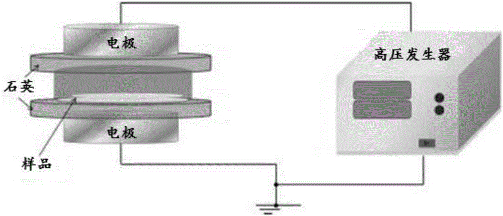
[0027] in such as figure 1 In the plasma processing device shown, the dielectric barrier discharge method is adopted at normal temperature and pressure, and a high-voltage generator is used to generate a voltage of 40 kV and a high frequency of 10 kHz to discharge in the cavity of the quartz reactor. The quartz reactor chamber was placed between two stainless steel electrodes with a distance of 8 mm. 1 gram of SBA-15 was evenly spread in a thin layer on the bottom of the reactor to ensure that all powders were subjected to plasma treatment with a similar ambient atmosphere. Oxygen was introduced, and under the condition of an output power of 110 watts, plasma was generated by dielectric barrier discharge, and the SBA-15 material was treated for 30 minutes. The treated material was recorded as SBA-15-O.
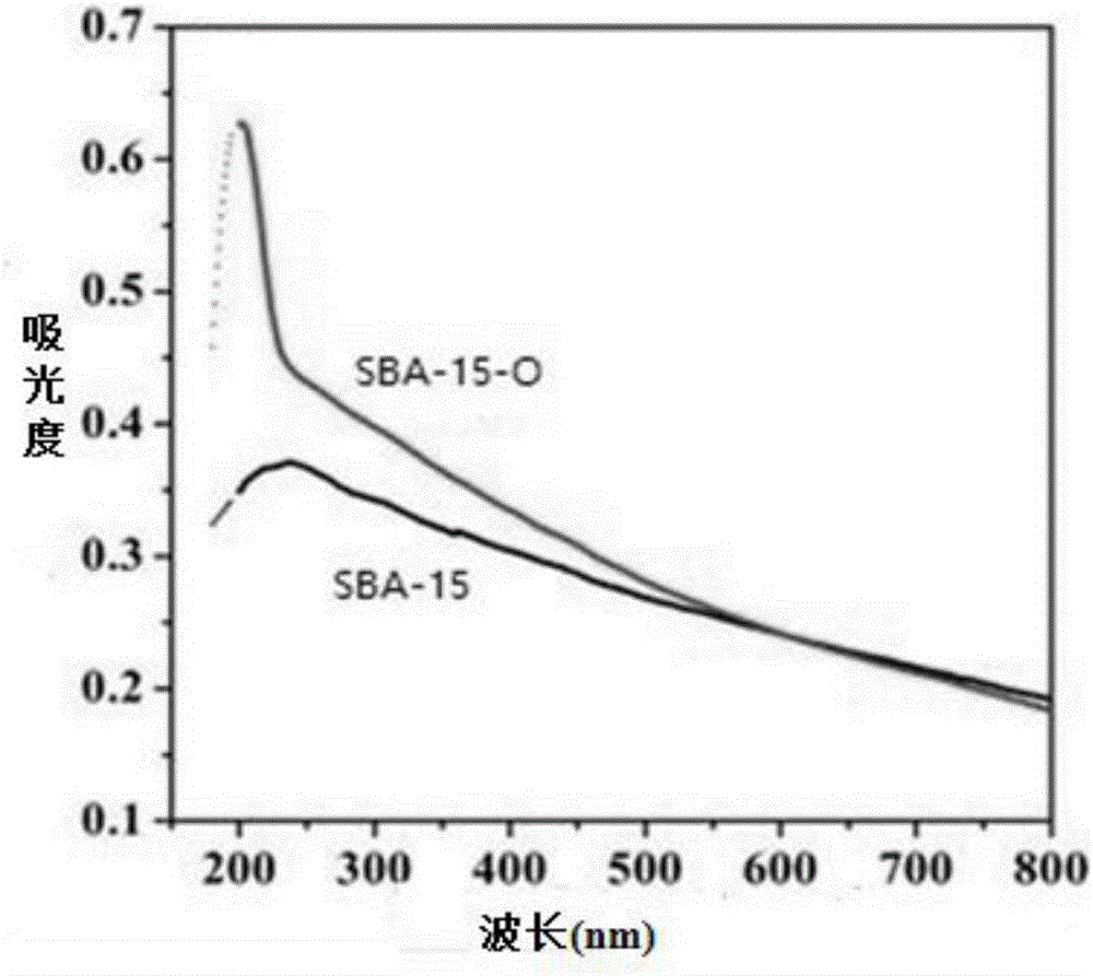
[0028] The UV spectra of SBA-15 before and after plasma treatment figure 2 As shown, the a...
Embodiment 2
[0029] Plasma treatment of SBA-15 under embodiment 2, trifluoromethane atmosphere
[0030] in such as figure 1 In the plasma processing device shown, dielectric barrier discharge is adopted at normal temperature and pressure, and a high-voltage generator is used to generate a voltage of 25 kV and a high frequency of 15 kHz to discharge in the cavity of the quartz reactor. The quartz reactor chamber was placed between two stainless steel electrodes with a distance of 10 mm. 1 gram of SBA-15 was evenly spread in a thin layer on the bottom of the reactor to ensure that all powders were subjected to plasma treatment with a similar ambient atmosphere. Introduce trifluoromethane gas, and under the condition of output power of 80 watts, plasma is generated by dielectric barrier discharge, and the SBA-15 material is processed for 40 minutes. The processed material is recorded as SBA-15-F.
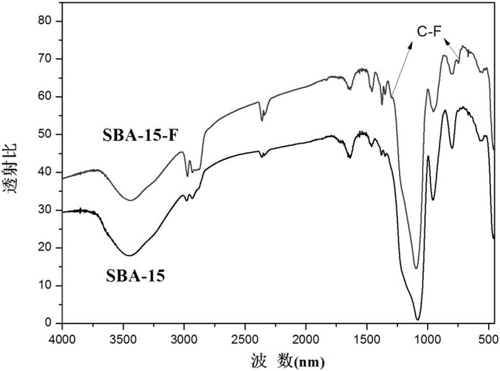
[0031] Infrared spectra of SBA-15 before and after plasma treatment image 3 As shown, the a...
PUM
| Property | Measurement | Unit |
|---|---|---|
| Height | aaaaa | aaaaa |
Abstract
Description
Claims
Application Information


