Manufacturing method of TFT backboard and TFT backboard

A manufacturing method and backplane technology, which are used in the manufacture of semiconductor/solid-state devices, electrical components, and electrical solid-state devices, etc., can solve the problems of uneven brightness, poor electron mobility, uneven distribution, etc., so as to improve the uniformity of light emission, Effects of low leakage current, improved electron mobility, and uniformity of current output

Active Publication Date: 2016-10-26
TCL CHINA STAR OPTOELECTRONICS TECH CO LTD
View PDF3 Cites 16 Cited by
  • Summary
  • Abstract
  • Description
  • Claims
  • Application Information

AI Technical Summary

Problems solved by technology

However, the ELA crystallization technology cannot effectively control the uniformity of the crystal lattice and the crystallization direction of the crystal lattice, so the distribution of crystallization on the entire substrate is very uneven, resulting in long-term inhomogeneity of the display effect and uneven brightness ( mura appears
[0006] Oxide Semiconductor (Oxide Semiconductor) is also a good material for TFT active layer. It has the characteristics of fast switching and low leakage current, but its electron mobility is slightly poor, which makes it slightly inferior in driving OLED

Method used


Image

  • Manufacturing method of TFT backboard and TFT backboard
  • Manufacturing method of TFT backboard and TFT backboard
  • Manufacturing method of TFT backboard and TFT backboard

Examples


Embodiment Construction

[0047] In order to further illustrate the technical means adopted by the present invention and its effects, the following describes in detail in conjunction with preferred embodiments of the present invention and accompanying drawings.

[0048] see figure 1 , the present invention at first provides a kind of manufacture method of TFT backplane, comprises the steps:

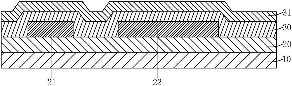
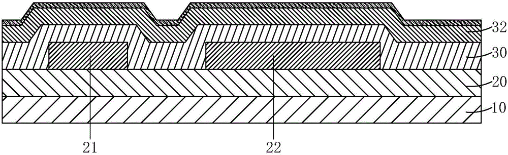
[0049] Step 1, such as figure 2 As shown, a base substrate 10 is provided, and a first gate 21 and a second gate 22 are formed at intervals on the base substrate 10, and the first gate 21, the second gate 22, and the A gate insulating layer 30 is deposited on the substrate 10 , and an amorphous silicon thin film 31 is deposited on the gate insulating layer 30 .

[0050] Specifically, the base substrate 10 is a glass substrate.

[0051] Specifically, the step 1 further includes: cleaning and baking the base substrate 10 before depositing other structural layers on the base substrate 10 .

[0052] Preferably, t...


PUM


Abstract

The invention provides a manufacturing method of a TFT backboard and the TFT backboard. A switching TFT is manufactured by an oxide semiconductor, so that the switching speed of the switching TFT is improved and the leakage current is reduced by the advantages that the oxide semiconductor is quick in switching and has relatively low leakage current. A drive TFT is manufactured by polycrystalline silicon, so that the electron mobility and the current output uniformity of the drive TFT are improved by the characteristics that the polycrystalline silicon has relatively high electron mobility and grain uniformity; and improvement of the light-emitting uniformity of an OLED device is facilitated.

Description

technical field [0001] The invention relates to the field of display technology, in particular to a method for manufacturing a TFT backplane and the TFT backplane. Background technique [0002] OLED (Organic Light-Emitting Diode, organic light-emitting diode) display, also known as organic electroluminescence display, is a new flat panel display device, because of its simple preparation process, low cost, low power consumption, high luminous brightness, Wide range of working temperature, light and thin size, fast response speed, easy to realize color display and large-screen display, easy to realize matching with integrated circuit driver, easy to realize flexible display, etc., so it has broad application prospects. [0003] According to the driving method, OLED can be divided into two categories: passive matrix OLED (Passive Matrix OLED, PMOLED) and active matrix OLED (Active Matrix OLED, AMOLED), namely direct addressing and thin film transistor matrix addressing. Among ...

Claims


Application Information

Patent Timeline
Patent Type & Authority Applications(China)
IPC IPC(8): H01L21/77H01L27/32
CPCH10K59/12H01L21/77H01L27/12
Inventor 张晓星周星宇徐源竣
Owner TCL CHINA STAR OPTOELECTRONICS TECH CO LTD
Why Eureka
Try Eureka