Tunneling field effect transistor capable of increasing current switching ratio
A technology of tunneling field effect and current switching ratio, which is applied in the direction of circuits, electrical components, semiconductor devices, etc., can solve the problems of deterioration of off-state current and increase of leakage current, and achieve high on-state current, high switching ratio, good Effect of Short Channel Characteristics
- Summary
- Abstract
- Description
- Claims
- Application Information
AI Technical Summary
Problems solved by technology
Method used
Image

Examples
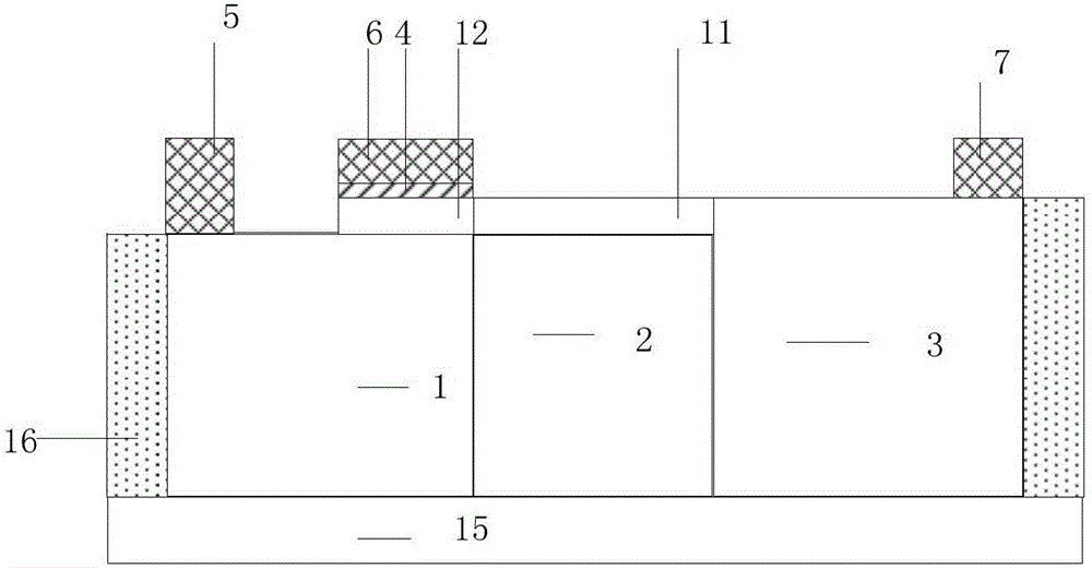
Embodiment 1
[0037] This example is for figure 1 The shown TFET device structure with increased current switching ratio takes an N-type TFET fabricated on a P-type substrate as an example. This embodiment does not include any method of increasing the on-state current and suppressing the off-state current, which is the simplest combination method.
[0038] The embodiment includes a source region 1, an intrinsic region 2, a drain region 3, a gate oxide layer 4, a source electrode 5, a gate electrode 6, a drain electrode 7, a conductive channel 11, an intrinsic region 12, a P-type high-resistance substrate 15, Isolation groove 16. First select the P-type doped bulk silicon of the (100) crystal plane for epitaxy, and then fabricate the PIN structure; or directly epitaxy a 20nm I layer on the P-type substrate, and then fabricate the PIN structure. Using ion implantation technology to implant B into the source region and implant P into the drain region respectively, to obtain P ++ source reg...
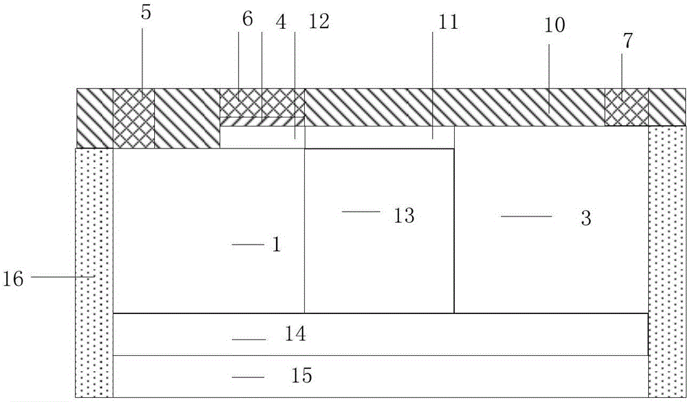
Embodiment 2
[0041] This example is for figure 2 The shown TFET device structure with increased current switching ratio takes an N-type TFET fabricated on a P-type substrate as an example. The N-type doped layer is in contact with the PIN structure above, and the thickness of the N-type doped layer is 200nm. Insulating low K dielectric uses SiO 2 N-type TFET, the relative permittivity is 3.9, and the high-K sidewall uses HfO with a relative permittivity of 22 2 . This embodiment includes all the ways of increasing the on-state current and suppressing the off-state current in the summary of the invention.
[0042] This embodiment includes a source region 1, a drain region 3, a gate oxide layer 4, a source electrode 5, a gate electrode 6, a drain electrode 7, sidewalls 10, a conductive channel 11, an intrinsic region 12, a low-K dielectric region 13, an N-type A doped layer 14, a P-type high-resistance substrate 15, and an isolation groove 16.
[0043] First select the P-type doped bulk ...
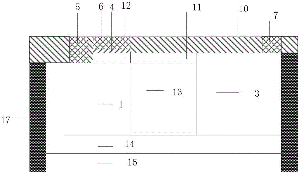
Embodiment 3
[0048] This example is for image 3 In the structure of the TFET device with increased current switching ratio shown, an N-type TFET fabricated on Si material is taken as an example. The insulating low-K medium adopts vacuum, and the relative permittivity is 1, that is, there is a cavity in the structure. The high-K sidewall adopts the method of directly depositing a passivation film. The N-type doped layer is in contact with the PIN structure above, and the thickness of the N-type buried layer is 200nm. In this embodiment, high-K dielectric and low-K dielectric are used to increase the on-state current, and PN junction isolation, low-K dielectric, and N-type doped layer are used to suppress the off-state current.
[0049] The embodiment includes source region 1, drain region 3, gate oxide layer 4, source electrode 5, gate electrode 6, drain electrode 7, sidewall 10, polysilicon 11, intrinsic region 12, low-K dielectric region 13, N-type buried layer 14. P-type high-resistan...
PUM
| Property | Measurement | Unit |
|---|---|---|
| Thickness | aaaaa | aaaaa |
| Thickness | aaaaa | aaaaa |
Abstract
Description
Claims
Application Information