Low-temperature wafer-level packaging method for lateral interconnection for RF mems device applications

A wafer-level packaging and device technology, which is applied to electric solid devices, semiconductor devices, and processes for producing decorative surface effects, etc., can solve the problem that the packaging strength and air tightness of organic materials cannot be guaranteed, and the process difficulty and process cost are increased. , Unable to realize the horizontal interconnection of leads, etc., to achieve the effect of strong plasticity, low cost and easy realization

Active Publication Date: 2017-08-11
SUZHOU XIMEI MICRO NANO SYST CO LTD
View PDF5 Cites 0 Cited by
  • Summary
  • Abstract
  • Description
  • Claims
  • Application Information

AI Technical Summary

Problems solved by technology

[0007] 1. In the existing technology, low-temperature packaging is easily limited by the substrate material, such as the anodic bonding packaging process, which requires sodium ion migration during the bonding process, which is usually only used for bonding between silicon-glass substrates ;Such as the surface activation low temperature bonding packaging process, usually only silicon-silicon direct bonding packaging can be achieved
[0008] 2. In the prior art, the low-temperature packaging process is easily limited by the flatness of the substrate surface, such as anodic bonding, Au / Si eutectic bonding, silicon-silicon bonding and other packaging processes, the flatness of the bonding surface usually requires Less than 1um, which greatly increases the difficulty and cost of the process
[0009] 3. In the existing technology, low-temperature packaging is not easy to pattern, such as surface activation low-temperature packaging technology
[0010] 4. In the prior art, the organic adhesive bonding packaging process can realize low-temperature packaging and lateral interconnection of leads, but the strength and airtightness of the organic material packaging cannot be guaranteed; although the metal packaging can guarantee the strength of the packaging and airtightness, but cannot realize the horizontal interconnection of leads, and must be combined with through-hole technology, which will inevitably increase the difficulty and cost of packaging

Method used


Image

  • Low-temperature wafer-level packaging method for lateral interconnection for RF mems device applications
  • Low-temperature wafer-level packaging method for lateral interconnection for RF mems device applications
  • Low-temperature wafer-level packaging method for lateral interconnection for RF mems device applications

Examples


Embodiment Construction

[0057] The specific implementation manners of the present invention will be further described in detail below in conjunction with the accompanying drawings and embodiments. The following examples are used to illustrate the present invention, but are not intended to limit the scope of the present invention.

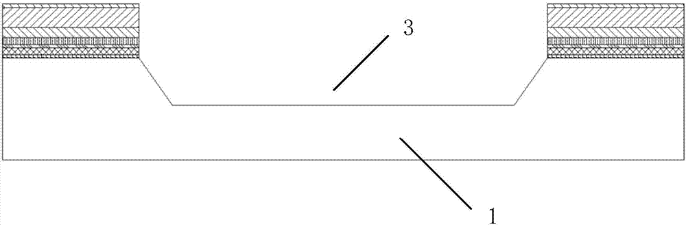
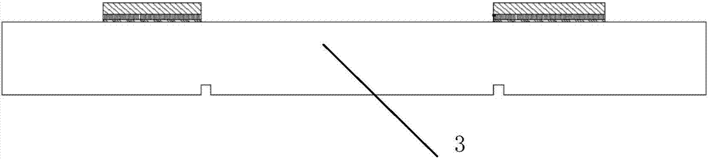
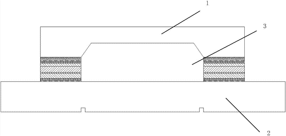
[0058] Such as Figures 1 to 4 The low-temperature wafer-level packaging method for lateral interconnection for the application of RF MEMS devices, which includes the fabrication of the package cover 1, the fabrication of the package substrate 2, and the alignment and bonding of the package cover 1 and the package substrate 2, which is unique at:

[0059] The fabrication of the package cover plate 1 includes the following steps:

[0060] First, choose a silicon wafer, or non-silicon material such as glass, or GaN, as the package cover material. After cleaning, a bonding wire pattern mask is photoetched.

[0061] Next, 20 to 50 nm of Ti is used as an adhesion layer by t...


PUM

PropertyMeasurementUnit
melting pointaaaaaaaaaa

Abstract

The invention relates to a transverse interconnection low-temperature wafer level packaging method specific to a radio-frequency MEMS (Micro Electro Mechanical System) device application. The method is characterized in that a low-temperature packaging process is performed on a radio-frequency device through a process which combines Au and In isothermal solidification low-temperature bonding with organic material bonding, so that the problem of lead transverse interconnection is solved, and high mechanical strength and airtightness are achieved during packaging at the same time. Meanwhile, a metal deposition way of Au and In isothermal solidification bonding is adopted, namely, Cu is taken as a barrier layer material for an Au and In isothermal solidification reaction, and a thin Au layer is deposited on a surface layer of an In layer to serve as a protection layer material for preventing the In surface layer from being oxidized. The manufacturing of a sealing ring mainly focuses on a packaging cover plate, so that the influence of packaging on the performance of a substrate chip is lowered greatly. Meanwhile, the manufacturing of the sealing ring and the manufacturing of a packaging cavity are integrated in process.

Description

technical field [0001] The invention relates to a low-temperature packaging method, in particular to a low-temperature wafer-level packaging method for lateral interconnection aimed at the application of radio frequency MEMS devices. Background technique [0002] It is the main goal of MEMS development to develop components or microsystems with new functions through miniaturization and high integration, so as to form a new technology industry field, and MEMS packaging plays a decisive role in the realization of this goal. Packaging is the most critical technology that determines the size, cost and reliability of commercial MEMS. RF MEMS device is a kind of MEMS device that requires extremely high packaging performance, and it is one of the key areas of MEMS packaging. At least one metal (gold or aluminum) is used as a structural material in RF MEMS devices, so the packaging of RF devices must be low-temperature packaging; since RF MEMS devices contain movable cantilever bea...

Claims


Application Information

Patent Timeline
Patent Type & Authority Patents(China)
IPC IPC(8): B81C1/00B81B7/00
CPCB81B7/0006B81B7/0032B81C1/00261B81C1/00269B81C1/00301
Inventor 刘泽文吴永强
Owner SUZHOU XIMEI MICRO NANO SYST CO LTD
Why Eureka
Try Eureka