Preparation and application of an organic-inorganic perovskite spike crystal
A technology of inorganic calcium and titanium ore, applied in the direction of crystal growth, single crystal growth, single crystal growth, etc., can solve the problem of difficult electron emission cathode, and achieve the effect of stable threshold field strength, low turn-on electric field, and stable emission
- Summary
- Abstract
- Description
- Claims
- Application Information
AI Technical Summary
Problems solved by technology
Method used
Image


Examples
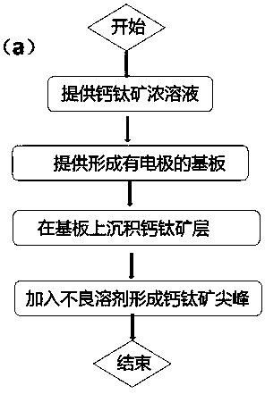
Embodiment 1
[0026] A method for preparing an organic-inorganic perovskite spike crystal, the specific steps are:
[0027] In the first step, an appropriate amount of CH 3 NH 3 I and PbI 2 The powder is dissolved in DMF solution to form a concentration of 50wt% concentrated solution; CH 3 NH 3 I and PbI 2 The molar ratio is 1:1; heating at 70°C for 12 hours under a nitrogen atmosphere to fully dissolve;
[0028] In the second step, a substrate 100 with electrodes 110 is provided, such as figure 2 As shown; the sputtered conductive glass with indium tin oxide is selected as the substrate electrode; in the atmospheric environment, it is sequentially ultrasonically cleaned by acetone, alcohol, and deionized water, and dried to obtain a clean conductive glass substrate of indium tin oxide;
[0029] In the third step, at room temperature, the perovskite solution prepared in the first step is scraped on the conductive glass substrate at a speed of 5 mm / s, and the wet thickness of the film...
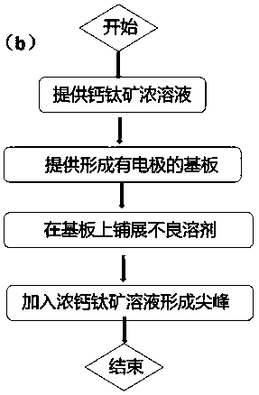
Embodiment 2
[0034] A method for preparing an organic-inorganic perovskite spike crystal, the specific steps are:
[0035] In the first step, an appropriate amount of CH 3 NH 3 I and PbI 2 The powder is dissolved in DMF solution to form a concentration of 50wt% concentrated solution; CH 3 NH 3 I and PbI 2 The molar ratio is 1:1; heating at 70°C for 12 hours under a nitrogen atmosphere to fully dissolve;
[0036] In the second step, a substrate 100 with electrodes 110 is provided, such as figure 2 As shown; the sputtered conductive glass with indium tin oxide is selected as the substrate electrode; in the atmospheric environment, it is cleaned by acetone, alcohol, and deionized water in sequence, and dried to obtain a clean conductive glass of indium tin oxide;
[0037] The third step, at room temperature, scrape the poor solvent chlorobenzene on the conductive glass;
[0038] The fourth step is to uniformly drop-coat the perovskite solution prepared in the first step on the poor so...
PUM
| Property | Measurement | Unit |
|---|---|---|
| thickness | aaaaa | aaaaa |
Abstract
Description
Claims
Application Information
 - R&D
- Intellectual Property
- Life Sciences
- Materials
- Tech Scout
- Unparalleled Data Quality
- Higher Quality Content
- 60% Fewer Hallucinations
Browse by: Latest US Patents, China's latest patents, Technical Efficacy Thesaurus, Application Domain, Technology Topic, Popular Technical Reports.
© 2025 PatSnap. All rights reserved.Legal|Privacy policy|Modern Slavery Act Transparency Statement|Sitemap|About US| Contact US: help@patsnap.com