Antimony-selenide thin-film solar battery using black phosphorene as conducting material and preparation method thereof

A technology of solar cells and conductive materials, applied in circuits, photovoltaic power generation, electrical components, etc., can solve the problems of cadmium being highly toxic, restricting development, and scarcity of tellurium resources

Active Publication Date: 2016-11-16
HUNAN NORMAL UNIVERSITY
View PDF2 Cites 8 Cited by
  • Summary
  • Abstract
  • Description
  • Claims
  • Application Information

AI Technical Summary

Problems solved by technology

For copper indium gallium selenide thin film solar cells, its photoelectric conversion efficiency has reached 21.7%, but its production process is complicated, and indium and gallium are expensive, and the production cost is high, which restricts its develop

Method used


Image

  • Antimony-selenide thin-film solar battery using black phosphorene as conducting material and preparation method thereof

Examples


Embodiment 1

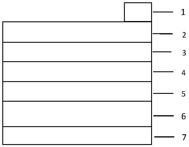
[0015] Embodiment 1: A kind of preparation method of antimony selenide thin-film solar cell using black phosphorene as conductive material, operate according to the following steps:

[0016] First, a p-type antimony selenide film was deposited on a p-type heavily doped black phosphorene substrate by a hydrazine solution method, and then an intrinsic hydrogenated nanocrystalline silicon film was prepared on a p-type antimony selenide film by plasma-enhanced chemical vapor deposition , and then use chemical vapor deposition to deposit n-type molybdenum disulfide film on the intrinsic hydrogenated nanocrystalline silicon film, then use chemical vapor deposition to deposit n-type heavily doped black phosphorene film on the n-type molybdenum disulfide film, and finally On the surface of the n-type heavily doped black phosphorene film and the p-type heavily doped black phosphorene substrate, metal silver electrodes are deposited respectively by screen printing, that is, the required ...

Embodiment 2

[0017] Example 2: First, a p-type antimony selenide thin film is deposited on a p-type heavily doped black phosphorene substrate by magnetron sputtering, and then the p-type antimony selenide thin film is prepared by plasma-enhanced chemical vapor deposition. Intrinsic hydrogenated nanocrystalline silicon film, and then deposit n-type molybdenum disulfide film on the intrinsic hydrogenated nanocrystalline silicon film by magnetron sputtering, and then deposit n-type heavily doped film on the n-type molybdenum disulfide film by mechanical exfoliation The black phosphorene thin film, and finally on the surface of the n-type heavily doped black phosphorene film and the p-type heavily doped black phosphorene substrate, metal aluminum electrodes are respectively deposited by vapor deposition, that is, the required black phosphorene as Antimony Selenide Thin Film Solar Cells of Conductive Materials.

Embodiment 3

[0018] Example 3: First, a p-type antimony selenide thin film is deposited on a p-type heavily doped black phosphorene substrate by an ultrasonic spray method, and then an intrinsic hydrogenation is prepared on a p-type antimony selenide thin film by plasma-enhanced chemical vapor deposition Nanocrystalline silicon film, and then deposit n-type molybdenum disulfide film on the intrinsically hydrogenated nanocrystalline silicon film by magnetron sputtering, and then deposit n-type heavily doped black film on the n-type molybdenum disulfide film by chemical vapor deposition. Phosphene thin film, and finally on the surface of the n-type heavily doped black phosphorene film and the p-type heavily doped black phosphorene substrate, metal silver electrodes are respectively deposited by evaporation method, that is, the required black phosphorene as the conductive material is obtained. Materials for antimony selenide thin film solar cells.


PUM


Abstract

The invention discloses an antimony-selenide thin-film solar battery using black phosphorene as a conducting material and a preparation method thereof. The solar battery is characterized in that the battery comprises a metal positive electrode 1, an n type heavily-doped black phosphorene film 2, an n type molybdenum disulfide 3, an intrinsic hydrogenated nano crystalline silicon film 4, a p type antimony selenide film 5, a p type heavily-doped black phosphorene substate 6, and a metal negative electrode 7. According to the invention, the solar battery has the following advantages: the molybdenum disulfide being a direct band-gap semiconductor material is used to form a buffer layer, the antimony selenide having a high absorptivity is used as absorption layer, the intrinsic hydrogenated nano crystalline silicon is used for realizing passivation of a pn junction interface, so that the defect-mode density of the interface is reduced; and because the black phosphorene is used as the conducting material, the series resistance of the battery is reduced, the light current is increased substantially, and the photoelectric conversion efficiency of the antimony-selenide thin-film solar battery is improved.

Description

technical field [0001] The invention belongs to the field of new energy, and in particular relates to an antimony selenide thin-film solar cell using black phosphorene as a conductive material and a preparation method thereof. Background technique [0002] In recent years, thin-film solar cells have increasingly become a research hotspot in the field of solar cells due to their advantages such as less raw material consumption, low energy consumption for preparation, and good product flexibility. For now, the technology in the field of thin-film solar cells is relatively mature, and the ones with relatively high photoelectric conversion efficiency mainly include copper indium gallium selenide thin-film solar cells and cadmium telluride thin-film solar cells. For copper indium gallium selenide thin film solar cells, its photoelectric conversion efficiency has reached 21.7%, but its production process is complicated, and indium and gallium are expensive, and the production cost...

Claims


Application Information

Patent Timeline
IPC IPC(8): H01L31/042H01L31/18
CPCH01L31/042H01L31/18H01L31/184Y02E10/544Y02P70/50
Inventor 罗云荣周如意陈春玲陈慧敏
Owner HUNAN NORMAL UNIVERSITY
Why Eureka
Try Eureka