Composite 3D printing method of buried circuit board

A 3D printing and circuit board technology, applied in the field of 3D printing, can solve the problems of not considering the assembly and arrangement of electronic components, the multi-layer circuit board does not have a groove structure, and is not suitable for mass production. The effect of removing restrictions and simplifying the structure

Active Publication Date: 2016-12-07
HUAZHONG UNIV OF SCI & TECH
View PDF12 Cites 34 Cited by
  • Summary
  • Abstract
  • Description
  • Claims
  • Application Information

AI Technical Summary

Problems solved by technology

[0005] However, further studies have shown that although the above-mentioned prior art proposes to use 3D printing technology to print circuit boards, it still has the following defects or deficiencies: First, the above-mentioned 3D printing technology uses layer-by-layer printing to print, and the prepared The multi-layer circuit board does not have a groove structure, and does not consider the assembly and arrangement of subsequent ele

Method used


Image

  • Composite 3D printing method of buried circuit board
  • Composite 3D printing method of buried circuit board

Examples


Embodiment 1

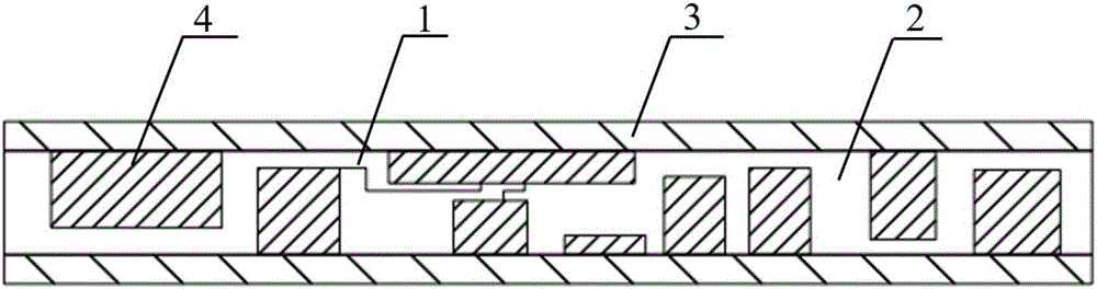
[0048] (1) Use 3D modeling software to design such as figure 1 The structural model of the embedded double-sided circuit board shown, in which 1 is the conductive circuit, 2 is the insulating substrate, 3 is the outer insulating board, and 4 is the electronic component; import the model file into the SLS / SLM forming device, and use the system slice The software slices the model in layers, each layer thickness is 0.03mm, and obtains the data information about the insulating substrate area, conductive line area and groove area in each layered slice;

[0049] (2) Place the nylon 6 powder in the powder feeding cylinder, and place the copper powder in the powder feeding nozzle of the coaxial suction / powder feeding mechanism with dual nozzles, wherein the nylon 6 powder is prepared by solvent precipitation method, and the particle size range is 10-30 μm , Copper powder is produced by gas atomization, the particle size range is 20-40μm, and both powders maintain good sphericity. The...

Embodiment 2

[0055] (1) Use 3D modeling software to design such as figure 1 The structural model of the embedded double-sided circuit board shown, in which 1 is the conductive circuit, 2 is the insulating substrate, 3 is the outer insulating board, and 4 is the electronic component; import the model file into the SLS / SLM forming device, and use the system slice The software slices the model in layers, each layer thickness is 0.01mm, and obtains the data information about the insulating substrate area, conductive line area and groove area in each layered slice;

[0056] (2) Place the nylon 12 powder in the powder feeding cylinder, and place the copper powder in the powder feeding nozzle of the coaxial suction powder feeding mechanism with dual nozzles, wherein the nylon 12 powder is prepared by solvent precipitation method, and the particle size range is 10-30 μm. Copper powder is produced by gas atomization, the particle size range is 20-40μm, and both powders maintain good sphericity. Th...

Embodiment 3

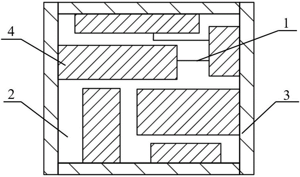
[0062] (1) Use 3D modeling software to design such as figure 2The structural model of the embedded four-sided circuit board is shown, in which 1 is the conductive circuit, 2 is the insulating substrate, 3 is the outer insulating board, and 4 is the electronic component. Import the model file into the SLS / SLM forming device, and use the system slicing software Carry out layered slices of the model, each layer thickness is 0.03mm, and obtain data information about the insulating substrate area, conductive line area and groove area in each layered slice;

[0063] (2) Nylon 12 powder is placed in the powder delivery tank, and copper-tin alloy powder is placed in the powder delivery nozzle of the coaxial suction powder delivery mechanism with dual nozzles. Nylon 12 powder is prepared by solvent precipitation method, and the particle size range is 15-35 μm , Copper powder is produced by gas atomization, the particle size range is 20-40μm, and both powders maintain good sphericity. ...


PUM

PropertyMeasurementUnit
Thicknessaaaaaaaaaa
Thicknessaaaaaaaaaa

Abstract

The invention belongs to the technical field of 3D printing, and particularly discloses a composite 3D printing method of a buried circuit board. Two 3D printing modes of selective laser melting (SLM) and selective laser sintering (SLS) are combined, an SLS/SLM forming device is used, selective distribution of insulation nonmetal powder and conductive metal powder in all layers in an insulation substrate area and a conducting circuit area is achieved through powder feeding spray heads and powder suction spray heads, and the groove-machining-free buried circuit board is manufactured through the main forming steps of modeling, slicing, powder spreading, powder suction, powder feeding and laser scanning forming. The advantages of being capable of forming complex shapes and micro structures of the 3D printing technology are utilized, integral manufacturing of the buried circuit board is achieved, the manufacturing process of a traditional buried circuit board is greatly simplified, the manufacturing cost is reduced, the manufacturing period is shortened, and the space utilization rate of the circuit board is remarkably increased.

Description

technical field [0001] The present invention relates to the technical field of 3D printing, more specifically, to a composite 3D printing method for embedded circuit boards, which can avoid groove processing and is suitable for integrated manufacturing, and is especially suitable for processing applications of embedded circuit boards or similar products occasion. Background technique [0002] Due to the gradual development of electronic products towards miniaturization and integration, the volume of circuit boards is constantly shrinking, and the number of electronic components is constantly increasing. The traditional method of manufacturing circuit boards is to arrange electronic components on the surface of the substrate, which cannot solve the contradiction between the reduction of the size of the circuit board and the increase of electronic components. Therefore, some researchers have proposed the idea of ​​embedding electronic components into the packaging substrate. ...

Claims


Application Information

Patent Timeline
IPC IPC(8): H05K3/30H05K3/00H05K1/18H05K1/02B29C67/00B22F3/105
CPCH05K1/0284H05K1/183H05K3/0014H05K3/30B33Y10/00B33Y40/00B22F10/00B22F10/362B22F12/55B22F12/53B22F10/28Y02P10/25
Inventor 史玉升王倩韩昌骏马高魏青松文世峰闫春泽宋波
Owner HUAZHONG UNIV OF SCI & TECH
Why Eureka
Try Eureka