Thin film resistor and manufacturing method thereof
A technology of thin film resistors and resistive layers, applied in thin film resistors, resistor manufacturing, resistors, etc., can solve problems such as increasing manufacturing costs and reducing surface roughness
- Summary
- Abstract
- Description
- Claims
- Application Information
AI Technical Summary
Problems solved by technology
Method used
Image
Examples
Embodiment 1
[0080] This embodiment relates to a metal thin film resistor.
[0081] First, glass with a thickness of 500 μm is selected as the substrate. Then, a resistance layer is formed on the surface of the glass substrate by adopting a treatment method of ion implantation followed by plasma deposition.
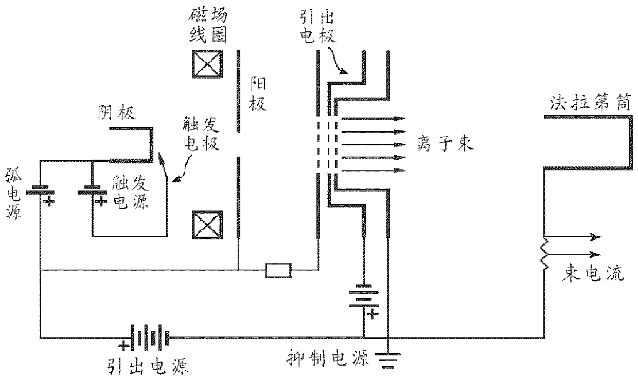
[0082] In the ion implantation process, one of Ti, Ta, Cr, Ni, Al, Cu, Ag, Au, V, Zr, Mo, Nb, In, Sn, Tb, Be, Ca, Mg is selected as the target material; Preferably, Ni or Cr can be selected as the vacuum cathode arc target material. Control the process temperature of ion implantation to 600°C, vacuumize to 2×10 -1 up to 5×10 -5 Pa, and adjust the energy of the implanted ions to 50-100keV, and the implanted dose is 1.0×10 17 to 5.0×10 17 ion / cm 2 , so that the lower surface of the ion implantation layer is located at a depth of 5-50 nm below the surface of the substrate.
[0083] In the plasma deposition process, one of Ti, Ta, Cr, Ni, Al, Cu, Ag, Au, V, Zr, Mo, Nb, In, Sn, Tb, ...
Embodiment 2
[0085] This embodiment relates to an alloy thin film resistor.
[0086] First, a silicon plate with a thickness of 80 μm is selected as the substrate. Then, a resistance layer is formed on the surface of the silicon plate by using a treatment method of ion implantation followed by plasma deposition. In the process of ion implantation and plasma deposition, the composition of the alloy target material used is shown in Table 1 below, where the values represent mass percentages.
[0087] components
Ni
Cr
Al
Ti
Cu
be
Ta
Au
Alloy combination 1
50
50
Alloy combination 2
40
40
20
Alloy combination 3
47
47
6
Alloy Set 4
75
15
10
Alloy combination 5
50
50
Alloy combination 6
30
20
15
10
25
Alloy combination 7
40
40
...
Embodiment 3
[0091] This embodiment relates to an alloy thin film resistor.
[0092] First, silicon dioxide with a thickness of 100 μm is selected as the substrate. Then, a resistance layer is formed on the surface of the silicon dioxide substrate by using a treatment method of ion implantation followed by plasma deposition.
[0093] In the process of ion implantation, different proportions of Ni-Cr alloys are selected and mixed with Ta, Al or Mo as the vacuum cathode arc target. Preferably, a Ni-Cr-dopant series alloy with a mass ratio of 40:40:20 or 35:55:10 is selected as the vacuum cathode arc target material, and the process temperature of ion implantation is controlled to be 600°C, and the vacuum is evacuated to 2 ×10 -1 up to 5×10 -5 Pa, and the energy of implanted ions is adjusted to 50 to 100keV, and the implanted dose is 1.0×10 17 to 5.0×10 17 ion / cm 2 , so that the lower surface of the ion implantation layer is located at a depth of 5-50 nm below the surface of the substra...
PUM
| Property | Measurement | Unit |
|---|---|---|
| thickness | aaaaa | aaaaa |
| thickness | aaaaa | aaaaa |
| thickness | aaaaa | aaaaa |
Abstract
Description
Claims
Application Information
 - R&D
- Intellectual Property
- Life Sciences
- Materials
- Tech Scout
- Unparalleled Data Quality
- Higher Quality Content
- 60% Fewer Hallucinations
Browse by: Latest US Patents, China's latest patents, Technical Efficacy Thesaurus, Application Domain, Technology Topic, Popular Technical Reports.
© 2025 PatSnap. All rights reserved.Legal|Privacy policy|Modern Slavery Act Transparency Statement|Sitemap|About US| Contact US: help@patsnap.com


