Array substrate, manufacturing method thereof, and display device

A manufacturing method and array substrate technology, which are applied in the fields of semiconductor/solid-state device manufacturing, electrical components, transistors, etc., can solve the problems of low process integration and high production cost

Inactive Publication Date: 2017-01-04
BOE TECH GRP CO LTD
View PDF2 Cites 15 Cited by
  • Summary
  • Abstract
  • Description
  • Claims
  • Application Information

AI Technical Summary

Problems solved by technology

However, at present, the manufacturing process of LTPS TFT and the manufacturing process of microcrystalline oxide TFT are carried out separately, the process integration degree is low, and the production cost is high.

Method used


Image

  • Array substrate, manufacturing method thereof, and display device
  • Array substrate, manufacturing method thereof, and display device
  • Array substrate, manufacturing method thereof, and display device

Examples


Embodiment 1

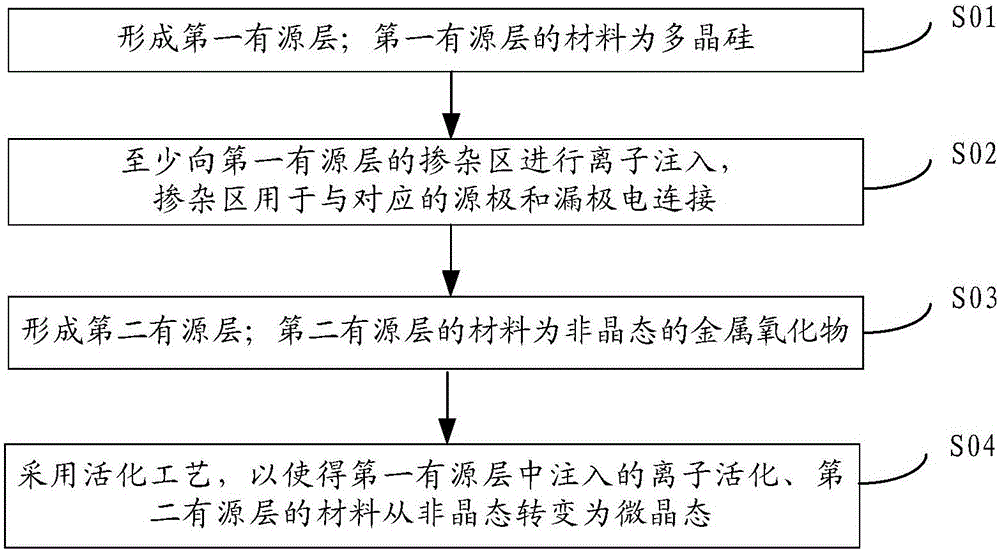
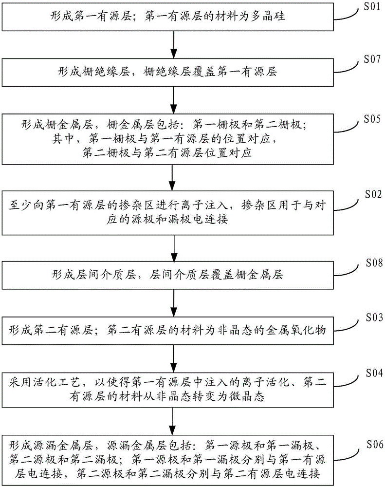
[0038] An embodiment of the present invention provides a method for manufacturing an array substrate, the method comprising:

[0039] S01, forming the first active layer; the material of the first active layer is polysilicon; the specific method for forming the first active layer is not limited here, as an example, an amorphous silicon film can be formed first, and then the amorphous silicon The film is irradiated with laser light to crystallize amorphous silicon (a-silicon) into polysilicon (p-silicon), forming a polysilicon film.

[0040] S02. Perform ion implantation at least into the doped region of the first active layer, the doped region is used for electrical connection with the corresponding source and drain; here, the method and type of implanted ions are not limited. As an example, boron ions can be implanted into the first active layer by plasma bombardment to form a P-type TFT; or, phosphorus ions can also be implanted into the first active layer by plasma bombardm...

Embodiment 2

[0060] An embodiment of the present invention provides an array substrate, which is formed by using any one of the manufacturing methods provided in the first embodiment. The array substrate has the characteristics of high process integration and low production cost. The array substrate may be a common array substrate or a COA (Color Filter on Array) substrate. The COA substrate refers to a substrate with a color filter layer on the array substrate, which is not limited here.

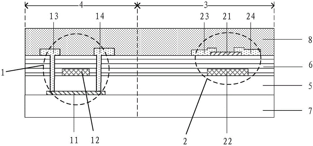
[0061] By adjusting the sequence of the fabrication method in Embodiment 1, array substrates with various structures can be formed. An array substrate with a specific structure is provided below. refer to figure 2 As shown, the array substrate includes: a substrate 7, a first active layer 11 sequentially arranged on the substrate 7, a gate insulating layer 5 covering the first active layer 11, a gate metal layer (the first gate 12 and The second gate 22), the interlayer dielectric layer 6 covering t...

Embodiment 3

[0063] An embodiment of the present invention provides a display device, including: the array substrate provided in Embodiment 2. The above-mentioned display device can be a display device such as a liquid crystal display, an electronic paper, an OLED (Organic Light-Emitting Diode, organic light-emitting diode) display, and any product with a display function such as a TV, a digital camera, a mobile phone, a tablet computer, etc. that include these display devices, or part. The display device has the characteristics of high process integration, low production cost, low power consumption and high stability. In addition, the size and application scenarios of the display device are not limited here; it can be a large-size display device, or a small-size, wearable display device, such as a bracelet, etc.; it can be applied indoors or Outdoors, since the display device has the characteristics of low power consumption, it is more advantageous to be applied outdoors.


PUM


Abstract

The invention provides an array substrate, a manufacturing method thereof, and a display device, which relate to the technical field of display. Through the manufacturing method of the array substrate, an ion activation process of LTPS TFT (Thin Film Transistor) and a process of converting an amorphous state of Oxide TFT into a mini-crystal state are integrated into a whole. The manufacturing method of the array substrate comprises the steps of forming a first active layer, wherein the material of the first active layer is polycrystalline silicon; at least carrying out ion implantation into a doping area of the first active layer, wherein the doping area is used for being electrically connected with a corresponding source electrode and a corresponding drain electrode; forming a second active layer, wherein the material of the second active layer is amorphous metallic oxide; after at least carrying out ion implantation into the doping area of the first active layer, and forming the second active layer, adopting an activation process so as to activate ion implanted into the first active layer and turn the material of the second active layer from the amorphous state to the mini-crystal state. The manufacturing method provided by the invention is applicable to manufacturing the array substrate and the display device comprising the array substrate.

Description

technical field [0001] The present invention relates to the field of display technology, in particular to an array substrate, a manufacturing method thereof, and a display device. Background technique [0002] Currently, outdoor wearable display devices are popular among users. In order to improve user experience, outdoor wearable display devices need to meet various requirements such as low power consumption, sensor integration, and narrow bezels. [0003] A display device generally includes: a packaging substrate and an array substrate. The array substrate is divided into a display area and a non-display area (also called a peripheral area) surrounding the display area; in the non-display area, LTPS TFT (Low Temperature Poly-silicon-Thin Film Transistor, Low Temperature Poly-silicon-Thin Film Transistor) technology is used to achieve narrow Frame and sensor circuit integration; in the display area, due to the amorphous Oxide TFT (Oxide Thin Film Transistor, oxide thin fi...

Claims


Application Information

Patent Timeline
Patent Type & Authority Applications(China)
IPC IPC(8): H01L21/77H01L21/265
CPCH01L21/265H01L21/77H01L21/425H01L27/092H01L27/1225H01L27/1251H01L27/1259H01L21/2652H01L27/1248H01L29/7869
Inventor 彭宽军廖峰
Owner BOE TECH GRP CO LTD
Why Eureka
Try Eureka