Manufacturing method of anti-PID battery piece and photovoltaic component

A battery sheet and equipment technology, applied in photovoltaic power generation, electrical components, circuits, etc., can solve problems such as rising electrical performance defect rate, loss of efficiency, and loss of benefits

Active Publication Date: 2017-01-11
CSG PVTECH +1
View PDF7 Cites 8 Cited by
  • Summary
  • Abstract
  • Description
  • Claims
  • Application Information

AI Technical Summary

Problems solved by technology

But the SiO formed in this way 2 The thickness, density and uniformity of the film cannot be guaranteed
Or by improving the cell SiN x The refractive index of the (silicon nitride layer) is used to achieve anti-PID, but it will cause Isc to drop and lose efficiency, and the electrical performance defect rate will increase, resulting in loss of benefit
[0003] In summary, the traditional solar cells have poor anti-PID performance

Method used


Image

  • Manufacturing method of anti-PID battery piece and photovoltaic component
  • Manufacturing method of anti-PID battery piece and photovoltaic component
  • Manufacturing method of anti-PID battery piece and photovoltaic component

Examples


preparation example Construction

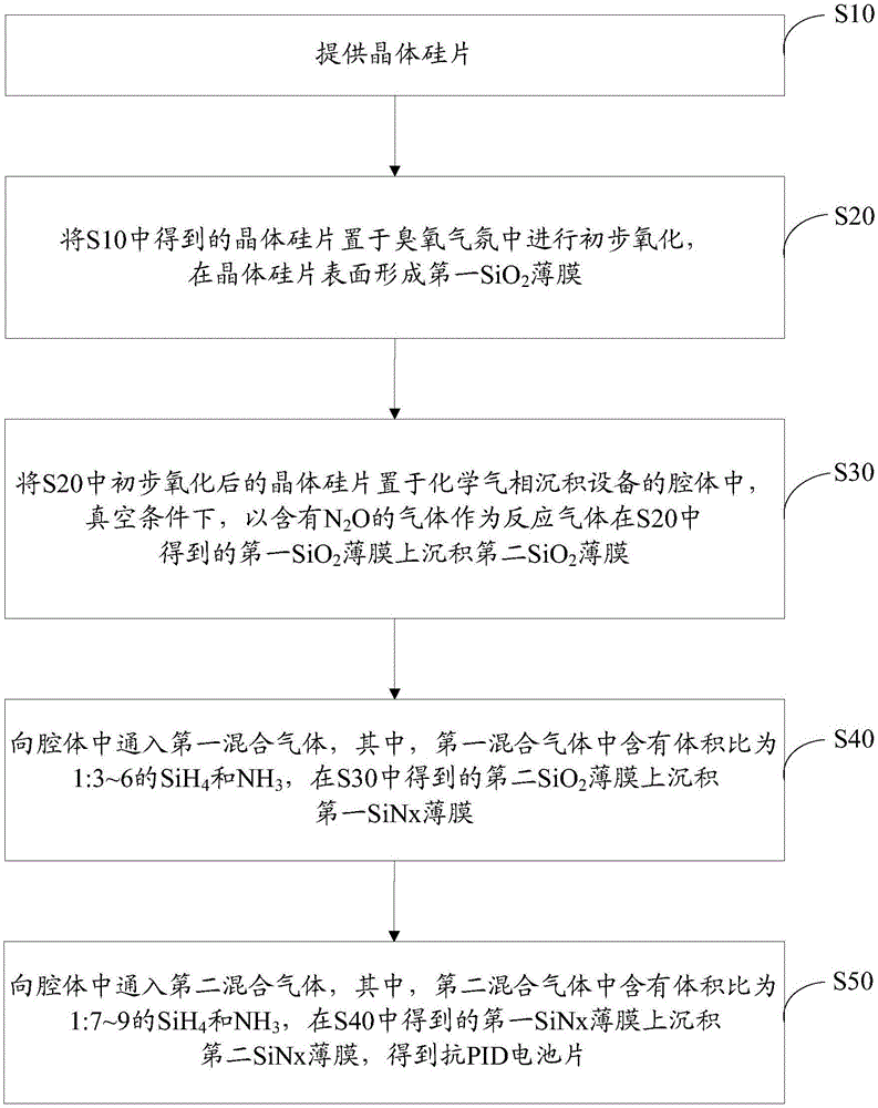
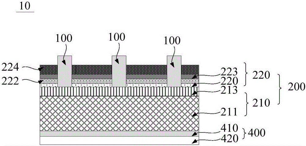
[0028] Such as figure 1 The preparation method of the anti-PID battery sheet of one embodiment shown, comprises the following steps:

[0029] S10, providing a crystalline silicon wafer.

[0030] In one embodiment, the crystalline silicon wafer may be a P-type polycrystalline silicon wafer.

[0031] In another embodiment, the crystalline silicon wafer may be an N-type polycrystalline silicon wafer.

[0032] In other embodiments, the crystalline silicon wafer may also be a single crystal silicon wafer or the like.

[0033] Specifically, before placing the crystalline silicon wafer in an ozone atmosphere for preliminary oxidation, pretreatment of the crystalline silicon wafer is also included, and the pretreatment includes texturing, diffusion and etching cleaning of the crystalline silicon wafer. After pretreatment, the oxidation of crystalline silicon wafers can be promoted, and the anti-PID performance of crystalline silicon wafers can be improved.

[0034] S20, placing th...

Embodiment 1

[0070] The P-type polysilicon wafer is sequentially subjected to conventional acid texturing and diffusion (forming a P-shaped region and an N-shaped region after diffusion), and then wet-etched and cleaned. Put the crystalline silicon wafer in the ozone oxidation equipment, pass oxygen into the ozone oxidation equipment, and oxidize the crystalline silicon wafer under the irradiation of ultraviolet light to form the first SiO2 on the surface of the crystalline silicon wafer. 2 film. Oxygen flow is controlled at 5 sccm, and compressed air flow is controlled at 10 sccm. First SiO 2 The thickness of the film is about 1 nm. Obtain the first SiO deposited on the surface of the crystalline silicon wafer 2 Thin film cells.

Embodiment 2

[0072] Adopt the same method as embodiment 1 to form the first SiO on the surface of crystalline silicon wafer 2 film. Then place the pre-oxidized crystalline silicon wafer in a tubular PECVD furnace tube, and vacuumize to maintain the vacuum degree in the cavity at about 1700mTor. Use N 2 Purge the crystalline silicon wafer after initial oxidation, and then pass N 2 O, the gas flow rate is 7000sccm, the reaction temperature is controlled at 450°C, the sputtering power is 5600W, and the coating time is about 100s. 2 A second SiO with a thickness of about 5 nm is deposited on the film 2 film. pump out the N in the cavity 2 O, keep the vacuum in the cavity at about 1600mTor, and pass the first mixed gas, SiH in the first mixed gas 4 The gas flow is 880sccm, NH 3 The gas flow rate is 3700sccm, the sputtering power is 6400W, and the coating time is about 150s. In the second SiO 2 Deposit the first SiN with a thickness of about 10nm on the film x film. Then pass into the ...


PUM

PropertyMeasurementUnit
thicknessaaaaaaaaaa
thicknessaaaaaaaaaa
thicknessaaaaaaaaaa

Abstract

The invention relates to a manufacturing method of an anti-PID battery piece and a photovoltaic component. The manufacturing method includes: putting a crystal silicon wafer in an ozone atmosphere for primary oxidation to form a first SiO2 thin film; using gas containing N2O as reaction gas to deposit a second SiO2 thin film on the first SiO2 thin film; depositing a first SiNx thin film in first mixed gas and a second SiNx thin film in second mixed gas. The second SiO2 thin film can make up incomplete coverage of primary oxidation and can increase thickness and compactness of a SiO2 film layer. Cooperation between the first SiNx thin film and the second SiNx thin film can enhance absorption of the surface of the battery piece to ultraviolet short waves. By the method, the battery piece is high in compactness of the film layer, more continuous in interface and good in anti-PID performance.

Description

technical field [0001] The invention relates to the field of batteries, in particular to a preparation method of an anti-PID battery sheet and a photovoltaic module. Background technique [0002] With the intensification of the global environmental and energy crisis, the cost of solar cell power generation continues to drop, and the application of photovoltaic power generation technology has been further promoted. Since the power generation income of solar cells is directly related to the service life, the concern about the long-term reliability of solar cell components during use is also increasing with the maturity of the market, among which the potential induced degardtion (PID) phenomenon Due to its ubiquity in commercial battery components, it has become a technical problem that the entire industry has to face and solve. The PID phenomenon refers to the fact that multiple groups of modules are connected in series outdoors to obtain a high voltage. Under the long-term h...

Claims


Application Information

Patent Timeline
Patent Type & Authority Applications(China)
IPC IPC(8): H01L31/0216H01L31/0236
CPCY02E10/50H01L31/02168H01L31/02167H01L31/02366
Inventor 吴娟梁杭伟李家兰叶雄新彭华
Owner CSG PVTECH
Why Eureka
Try Eureka