Perovskite solar cell containing hydrophilic electrode modification layer and preparation method
A technology of electrode modification layer and solar cell, which is applied in the direction of circuits, photovoltaic power generation, electrical components, etc., can solve the problems of poor device stability and fast attenuation speed, achieve improved stability, improve light stability, increase photocurrent and photoelectricity The effect of conversion efficiency
- Summary
- Abstract
- Description
- Claims
- Application Information
AI Technical Summary
Problems solved by technology
Method used
Image

Examples
Embodiment 1
[0040] A conventional perovskite solar cell device (reference device)
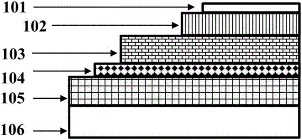
[0041] like figure 1 A schematic diagram of the device structure of a perovskite solar cell with a traditional structure without a hydrophobic electrode modification layer is shown, from bottom to top are counter electrode gold (Au), hole transport layer (Spiro-OMeTAD), calcium Titanium active layer (CH 3 NH 3 PB 3 ), electron transport layer (Nb-TiO 2 ) and FTO conductive glass substrate. The hole transport layer has a thickness of 100-300nm, the perovskite active layer has a thickness of 300-600nm, the electron transport layer has a thickness of 30-50nm, and the FTO transparent conductive substrate has a thickness of 400-800nm. Its preparation process is as follows:
[0042] (1) Preparation of a transparent conductive glass substrate: In this embodiment, a commercial FTO transparent conductive substrate is used, and the average transmittance is 85%. The FTO substrate was ultrasonically cleaned wit...
Embodiment 2
[0048] Fabrication of a Perovskite Solar Cell Device Containing a Hydrophobic Electrode Modification Layer
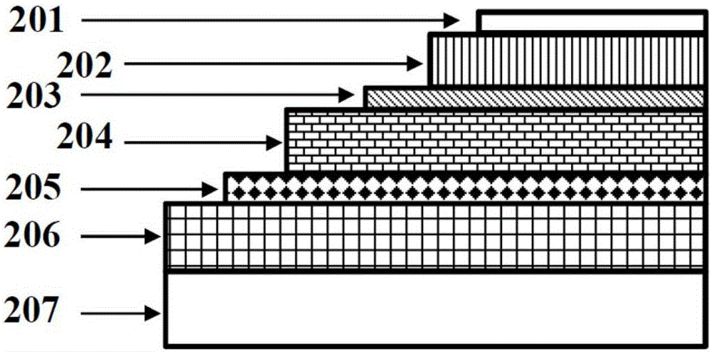
[0049] like figure 2 A schematic diagram of the device structure of a perovskite solar cell containing a hydrophobic electrode modification layer is shown, a perovskite solar cell containing a hydrophobic electrode modification layer, from bottom to top is the counter electrode gold (Au), Hole transport layer (Spiro-OMeTAD), hydrophobic electrode modification layer (ZnPc), perovskite active layer (CH 3 NH 3 PB 3 ), electron transport layer (5% Nb-TiO 2 ) and FTO conductive glass substrate; the hydrophobic electrode modification layer is zinc phthalocyanine.
[0050] The thickness of the hole transport layer is 100-300nm, the thickness of the hydrophobic electrode modification layer is 40-100nm, the thickness of the perovskite active layer is 300-600nm, the thickness of the electron transport layer is 30-50nm, FTO transparent The conductive substrate has a thicknes...
PUM
| Property | Measurement | Unit |
|---|---|---|
| Thickness | aaaaa | aaaaa |
| Thickness | aaaaa | aaaaa |
| Thickness | aaaaa | aaaaa |
Abstract
Description
Claims
Application Information
 - Generate Ideas
- Intellectual Property
- Life Sciences
- Materials
- Tech Scout
- Unparalleled Data Quality
- Higher Quality Content
- 60% Fewer Hallucinations
Browse by: Latest US Patents, China's latest patents, Technical Efficacy Thesaurus, Application Domain, Technology Topic, Popular Technical Reports.
© 2025 PatSnap. All rights reserved.Legal|Privacy policy|Modern Slavery Act Transparency Statement|Sitemap|About US| Contact US: help@patsnap.com