Method and device for reducing metal microwire and/or nanowire network electrode resistance

A technology of metal nanowires and electrode resistance, which is applied in the direction of nanotechnology, nanotechnology, nanotechnology, etc. for materials and surface science, can solve the pollution of metal microwires and nanowires, the chemical method is difficult to control the processing intensity, and consumes a lot of energy Chemical and other problems, to achieve the effect of simple and efficient processing, low cost, and low cost

Active Publication Date: 2020-05-19
HUAZHONG UNIV OF SCI & TECH
View PDF4 Cites 0 Cited by
  • Summary
  • Abstract
  • Description
  • Claims
  • Application Information

AI Technical Summary

Problems solved by technology

Compared with traditional oxide transparent conductive electrodes, metal microwires and / or nanowires have higher conductivity, and nanowire networks have outstanding advantages such as high transmittance and can be used in flexible and stretchable devices. However, due to The unavoidable organic coating during the synthesis of metal microwires and / or nanowires leads to the assembly of metal microwires and / or nanowire network electrodes into a transparent network after spraying, contact or non-contact printing or drop coating, etc. There is often a large node contact resistance
[0003] Existing methods for reducing the resistance of such electrodes mainly include high-temperature heat treatment, mechanical imprinting, plasma treatment, and chemical wet etching, all of which consume a lot of energy or produce a lot of chemical pollutants. In particular, it is difficult to master the treatment intensity by chemical methods, which can easily cause contamination of metal micro-wires and / or nano-wires, making cleaning difficult

Method used


Image

  • Method and device for reducing metal microwire and/or nanowire network electrode resistance
  • Method and device for reducing metal microwire and/or nanowire network electrode resistance
  • Method and device for reducing metal microwire and/or nanowire network electrode resistance

Examples


Embodiment 1

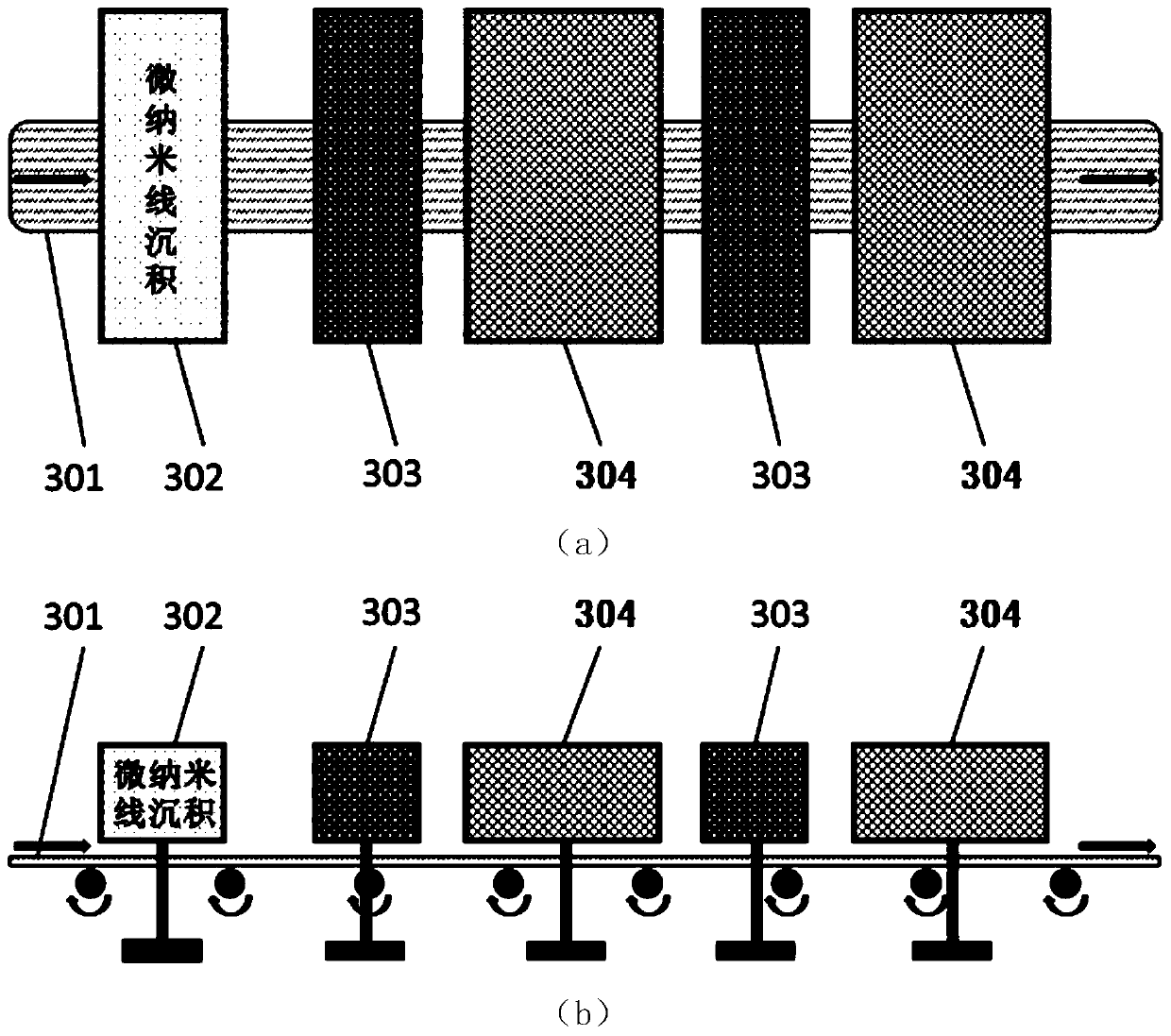
[0051] This embodiment provides a device for quickly reducing the resistance of metal microwires and / or nanowire network electrodes, and its structural schematic diagram is as follows image 3 As shown, the device includes a transfer unit 301 , a deposition unit 302 , two wetting units 303 and two drying units 304 .

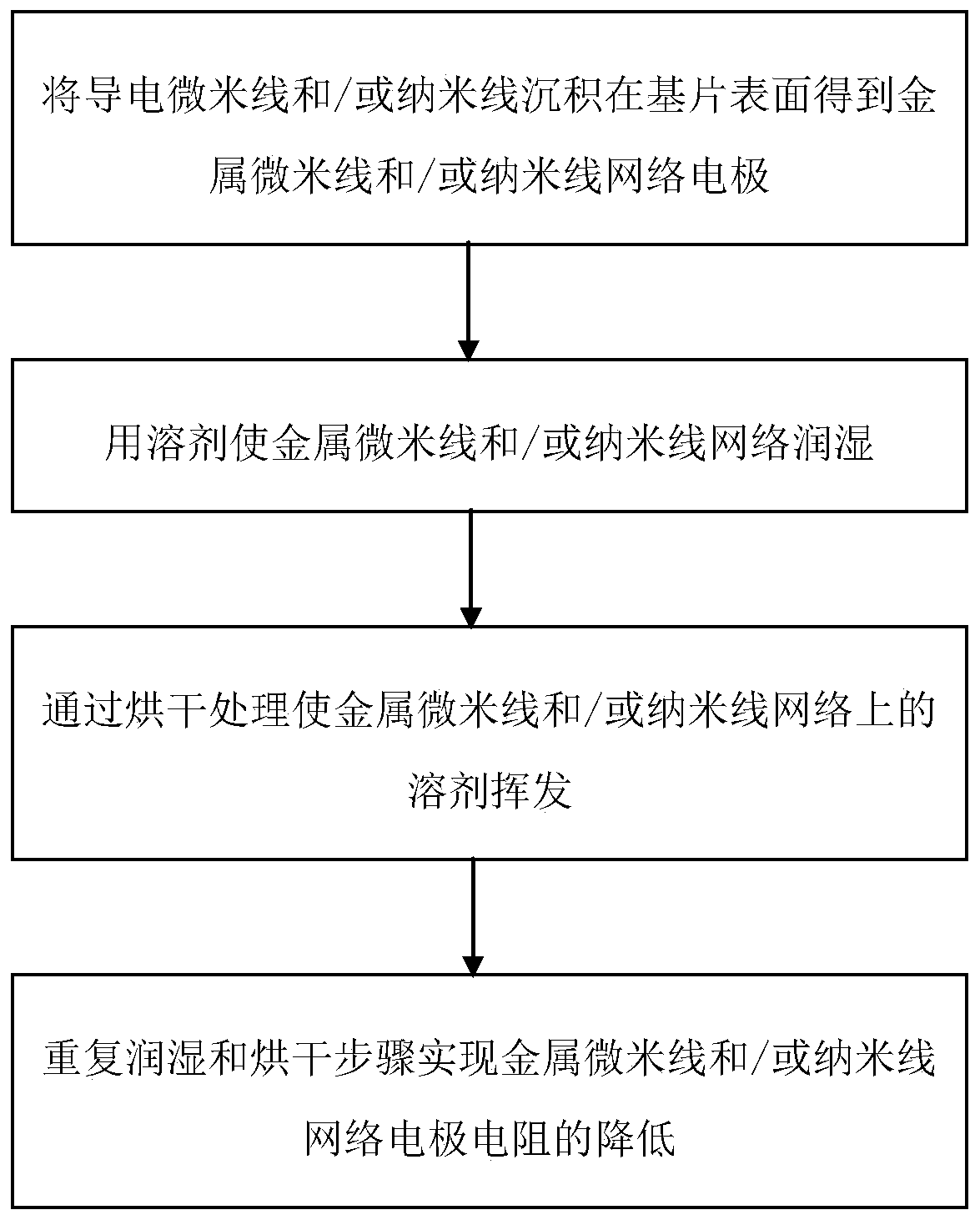
[0052] The transfer unit 301 communicates with other units in the device, and sends the substrate from the starting position to the metal microwire and / or nanowire deposition unit 302 for deposition, by means of contact or non-contact printing, spray coating or spin coating, Deposit the conductive nanowires on the surface of the substrate to form a network, and then continue to send the substrate with the metal microwires and / or nanowire network electrodes deposited on the surface into the wetting unit 303 to conduct the metal microwires and / or nanowire network electrodes. Wetting, and finally the solvent is dried by the drying unit 304; after a round of "wetting...

Embodiment 2

[0054] This embodiment provides another device for quickly reducing the resistance of metal microwires and / or nanowire network electrodes, and its structural schematic diagram is as follows Figure 4 As shown, the device includes a conveying unit 401 , a deposition unit 402 , two wetting units 403 , two drying units 404 and two direction-controllable conveying subunits 405 .

[0055] The transfer unit 401 communicates with all other units in the device, and sends the substrate from the initial position to the metal microwire and / or nanowire deposition unit 402 for deposition, by means of contact or non-contact printing, spray coating or spin coating , deposit conductive nanowires on the surface of the substrate to form a network, and then continue to send the substrate with metal microwires and / or nanowire network electrodes deposited on the surface into the wetting unit 403 for metal microwires and / or nanowire network electrodes Wetting, and then drying the solvent through th...


PUM

PropertyMeasurementUnit
diameteraaaaaaaaaa

Abstract

The invention discloses a method and apparatus reducing the resistance of metal micrometer wire and / or nanowire network electrodes. The method comprises the step of firstly depositing metal micrometer wires and / or nanowires on the surface of a substrate, and then wetting a metal micrometer wire and / or nanowire network with a solvent, subjecting the network to drying to volatilize the solvent, and finally repeating wetting and drying to realize the lowering of the resistance of the metal micrometer wire and / or nanowire network electrodes. The apparatus comprises a deposition unit for depositing the metal micrometer wires and / or nanowires on the surface of the substrate, a wetting unit for wetting the metal micrometer wire and / or the nanowire network electrodes, a drying unit for volatilizing the surface solvent of the micrometer wire and / or the nanowire network electrodes and a transfer unit for transporting substrates and the metal micrometer wire and / or the nanowire network electrodes between the wetting unit and the drying unit. The method and apparatus of the invention can greatly reduce the resistance of the metal micrometer wire and / or the nanowire network electrodes, and has advantages such as rapidness, high efficiency, low cost, no pollution, etc.

Description

technical field [0001] The invention belongs to the technical field of preparation and processing of micro-nano functional structures / materials, and more specifically relates to a method and device for rapidly reducing the resistance of metal micro-wire and / or nano-wire network electrodes. Background technique [0002] With the rapid development of the controllable growth technology of nanomaterials in recent years, many materials have gradually developed from the micrometer scale to the nanometer scale, and the application of micro-nanomaterials in many fields today is becoming more and more extensive. Among them, one-dimensional or quasi-one-dimensional The application of metal microwires and / or nanowires on transparent thin film electrodes has great potential, and the synthesis of metal microwires and / or nanowires and the preparation process of transparent network electrodes have become increasingly mature. Compared with traditional oxide transparent conductive electrodes...

Claims


Application Information

Patent Timeline
Patent Type & Authority Patents(China)
IPC IPC(8): H01L21/28B82Y30/00H01L21/67
CPCB82Y30/00H01L21/28H01L21/67011
Inventor 周军胡彬李嘉张奎
Owner HUAZHONG UNIV OF SCI & TECH
Why Eureka
Try Eureka