Copper alloy bonding wire

A technology of copper alloy and bonding wire, applied in the direction of semiconductor/solid-state device components, semiconductor devices, electrical components, etc., to achieve stable position, shorten the time of bonding steps, and stabilize the shape

Inactive Publication Date: 2017-03-08
TANAKA DENSHI KOGYO KK
View PDF15 Cites 2 Cited by
  • Summary
  • Abstract
  • Description
  • Claims
  • Application Information

AI Technical Summary

Problems solved by technology

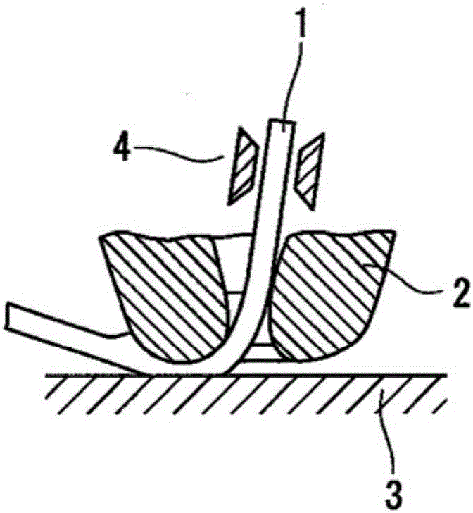
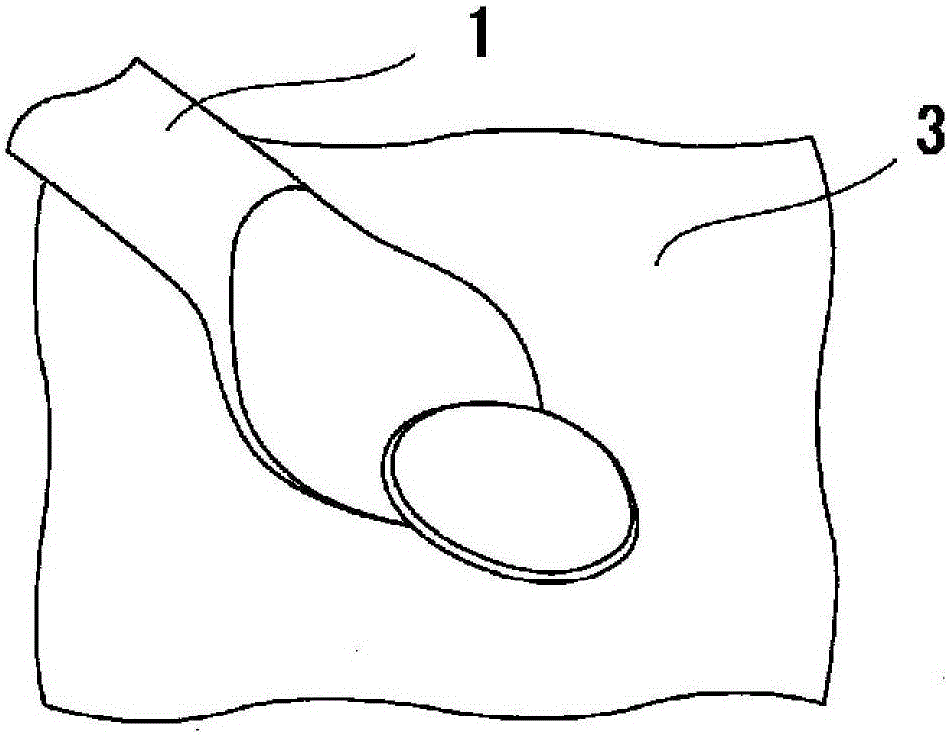
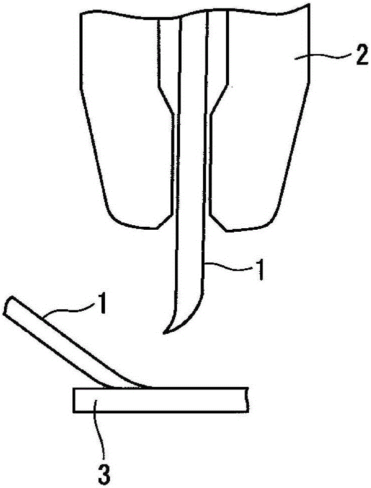
[0018] The present invention is used to solve the following technical problem: in the wedge welding step of pulling up the copper alloy bondi

Method used


Image

  • Copper alloy bonding wire
  • Copper alloy bonding wire
  • Copper alloy bonding wire

Examples


Embodiment

[0062] The core material is copper (Cu) with a purity of 99.9998 mass % (5N), phosphorus (P), nickel (Ni), palladium (Pd), platinum (Pt), gold (Au) and silver (Ag) as an added element. As the base metal element, an element generally contained in high-purity copper is selected. That is, bismuth (Bi), selenium (Se), tellurium (Te), zinc (Zn), iron (Fe), nickel (Ni), and tin (Sn) are appropriately selected. Embodiments in which these metals are blended within a given range are referred to as Example 1 to Example 5, respectively.

[0063] Next, this was dissolved and continuously casted, and then the first wire drawing was performed within the range of 95 to 99.99% or less of the cross-sectional reduction rate to obtain a thick wire (diameter 1.0 mm) before coating the drawn material. Next, intermediate heat treatment (treatment at 300-600° C. for 0.5-3 hours) was performed (Example 4, Example 5) or no intermediate heat treatment was performed (Example 1-Example 3). Afterwa...


PUM


Abstract

The invention provides a copper alloy bonding wire, wherein the number of copper alloy grains in unit cross area is 50-250, and a highest grain particle is less than one third of diameter of the bonding wire. Furthermore the copper alloy grains has no directionality, wherein the proportion of the copper alloy grains in a specific direction is lower than 40%.

Description

technical field [0001] The present invention relates to a copper alloy bonding wire suitable for connecting an IC chip electrode used in a semiconductor device to a substrate such as an external lead frame. Background technique [0002] In general, a method called ball bonding is used for the first bonding of copper bonding wires and electrodes, and a method called wedge bonding is used for copper bonding wires and wirings on a circuit wiring board for semiconductors. for wedge welding. In the first bonding, a thermal arc is applied from a torch electrode to the tip of the wire by an electronic frame off (EFO) method to form a positive ball called a solder ball (FAB) at the tip of the wire. Next, ultrasonic waves (ultrasonic waves) were applied while pressing the FAB on the aluminum pad heated in the temperature range of 150 to 300° C. with a capillary to bond the bonding wire to the aluminum pad. [0003] Next, while pulling out the bonding wire, the solder pin is raised,...

Claims


Application Information

Patent Timeline
IPC IPC(8): H01L23/49H01L23/498
CPCH01L23/49811H01L24/45H01L23/49H01L2224/45139H01L2224/45147H01L2224/45144H01L2224/45163H01L2224/78301H01L2224/85H01L2924/00011H01L2224/45565H01L2224/45572H01L2224/45644H01L2224/45664H01L2224/48247H01L2224/48451H01L2224/48456H01L2224/85439H01L2224/43848H01L2924/01079H01L2924/01047H01L2924/01015H01L2924/01028H01L2924/01046H01L2924/01078H01L2924/013H01L2924/01026H01L2924/0103H01L2924/01034H01L2924/0105H01L2924/01052H01L2924/01083H01L2924/00013H01L2924/01033H01L2924/01206H01L2924/01049
Inventor 天野裕之三苫修一滨本拓也
Owner TANAKA DENSHI KOGYO KK
Why Eureka
Try Eureka