Method for producing crystal bars

A production method and a technology for crystal rods, which are applied in chemical instruments and methods, single crystal growth, single crystal growth and other directions, can solve the problems of unable to achieve ideal results, unable to meet wafer consistency requirements, poor annealing effect, etc. Conducive to popularization and application, high internal stress consistency, and the effect of eliminating residual stress

Active Publication Date: 2017-03-29
FUJIAN JING AN OPTOELECTRONICS CO LTD
View PDF8 Cites 2 Cited by
  • Summary
  • Abstract
  • Description
  • Claims
  • Application Information

AI Technical Summary

Problems solved by technology

[0005] As another example, in the prior art, annealing is performed after cutting the wafer. Although the warpage can be improved to a certain extent and the stress is released, the annealing effect is not good at this time because the wafer has been separated from the ingot, which cannot meet the requirements of the wafer. Consistency requirements
On the whole, the existing technology cannot achieve the desired effect

Method used


Image

  • Method for producing crystal bars
  • Method for producing crystal bars
  • Method for producing crystal bars

Examples


Embodiment 1

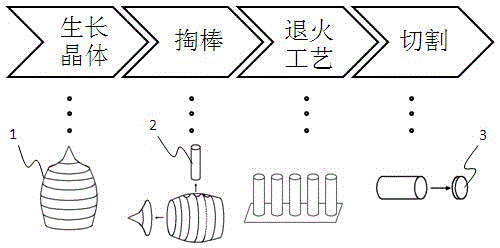
[0035] see figure 1 Shown, a kind of manufacture method that is used for sapphire ingot of the present invention specifically comprises the following steps:

[0036] Step 1: In this embodiment, Kyropoulos Method, heat exchange method (HEM method), guided mode method (EFG) and other methods can be used for crystal growth. During the crystal growth process, due to the control of the growth rate, the change of the temperature gradient in the chamber needs to be strictly controlled, and as the volume of the crystal increases, the change of the internal temperature field becomes more complicated.

[0037] This embodiment is preferably the Kyropoulos method, which is divided into stages such as seeding, shouldering, growth, and cooling. The growth temperature and heat flow field changes in each stage are different, and the internal residual stress is also different; especially different In order to reduce the cost of the crystal 1, the growth cycle is shortened, as long as the crys...

Embodiment 2

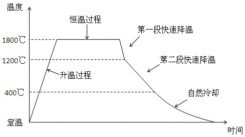
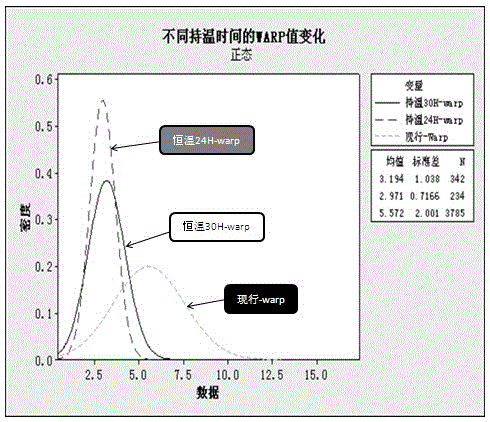
[0047] The present invention also provides a manufacturing method for silicon carbide crystal 1 to produce wafer 3, which solves the warping problem of silicon carbide wafer 3. Step 1, grows silicon carbide crystal 1, does not limit the growth process of silicon carbide crystal 1, in silicon carbide After the crystal 1 is drawn into a crystal rod, the silicon carbide crystal rod 2 is annealed, because silicon carbide will decompose at about 1850°C, so compared with Example 1, the highest temperature during the heating process of the silicon carbide crystal rod 2 is Set to 1700°C~1800°C. Maintain a uniform heating rate during the heating process, and the heating rate is 50 ° C ~ 200 ° C. After reaching the highest temperature, it enters the constant temperature process, and the constant temperature process time is 3h~32h. After the constant temperature process is over, rapid cooling begins. The rapid cooling speed is 50°C~200°C. When the temperature cools to 350~450°C, it ente...

Embodiment 3

[0050] The difference between this embodiment and embodiment 2 is that the material of the ingot is gallium arsenide. Since the melting point of gallium arsenide is lower than that of silicon carbide, the melting point is 1238°C, so the maximum temperature in the heating process is set at 900°C~1150°C. It is preferably 900°C~1050°C, and its heating rate, constant temperature process and rapid cooling process are similar to those of silicon carbide crystals. Crystal rods can also be produced by the method of the present invention.


PUM


Abstract

The invention discloses a method for producing crystal bars. The method is characterized in that before online cutting, crystal bars which are treated by a bar picking technology are placed in a high temperature annealing furnace for carrying out annealing; the annealing process mainly comprises the following step: a heating process, a constant temperature process, and a cooling process. The annealing process method of sapphire crystal bars is provided, unified annealing processing is carried out for crystal bars produced by different crystal growths and bar picking technology, residual stress in the crystal bars is eliminated, consistency of the quality of sapphire crystal bars is improved, and posterior wafer processing, and epitaxial yield rate and uniformity are improved.

Description

technical field [0001] The invention relates to a method for manufacturing crystal rods, in particular to an annealing method for crystal rods. Background technique [0002] Sapphire (α-Al 2 o 3 ) crystal has excellent characteristics such as high hardness, high melting point, good light transmittance, good thermal stability and stable chemical properties. It is widely used in national defense, aerospace, industry and life fields, especially suitable as LED the substrate material. At present, sapphire substrates account for more than 95% of semiconductor lighting substrates. The quality of the sapphire substrate (referred to as the substrate) has a great influence on the growth of the subsequent GaN epitaxial layer and the performance and yield of the blue light diode. The production of high-quality LED products must first ensure the quality of the substrate. quality. [0003] As a crystal material for making LED substrates, sapphire ingots are in great demand. The gro...

Claims


Application Information

Patent Timeline
Patent Type & Authority Applications(China)
IPC IPC(8): C30B33/02C30B29/20C30B29/36C30B29/42
CPCC30B29/20C30B29/36C30B29/42C30B33/02
Inventor 谢斌晖胡中伟林武庆赖柏帆廖桂芬
Owner FUJIAN JING AN OPTOELECTRONICS CO LTD
Why Eureka
Try Eureka