Supercharge Your Innovation With Domain-Expert AI Agents!

Improved structure of copper metal on the backside of semiconductor element

A backside metal and improved structure technology, applied in semiconductor devices, semiconductor/solid-state device components, electrical components, etc., can solve problems such as unsatisfactory high temperature resistance, damage, and damage to semiconductor components

Active Publication Date: 2019-08-27
WIN SEMICON
View PDF6 Cites 0 Cited by
  • Summary
  • Abstract
  • Description
  • Claims
  • Application Information

AI Technical Summary

Problems solved by technology

[0003] However, tantalum nitride (TaN) is used as the diffusion barrier layer, gold (Au) is used as the stress relief metal layer, and copper (Cu) is used as the back metal layer. The performance of the operation is not ideal; the heat dissipation and high temperature resistance of semiconductor components are very important issues nowadays. If the high temperature resistance of the components is not ideal, the semiconductor components may be damaged due to overheating, especially when the semiconductor components have backside conductors. In the case of holes, the aspect ratio of the backside guide holes is usually very large. Under high temperature operation, the three-layer structure is more likely to produce voids, cracks, peeling, etc., resulting in poor grounding and damage to the semiconductor element.

Method used


Image

  • Improved structure of copper metal on the backside of semiconductor element
  • Improved structure of copper metal on the backside of semiconductor element
  • Improved structure of copper metal on the backside of semiconductor element

Examples


Embodiment Construction

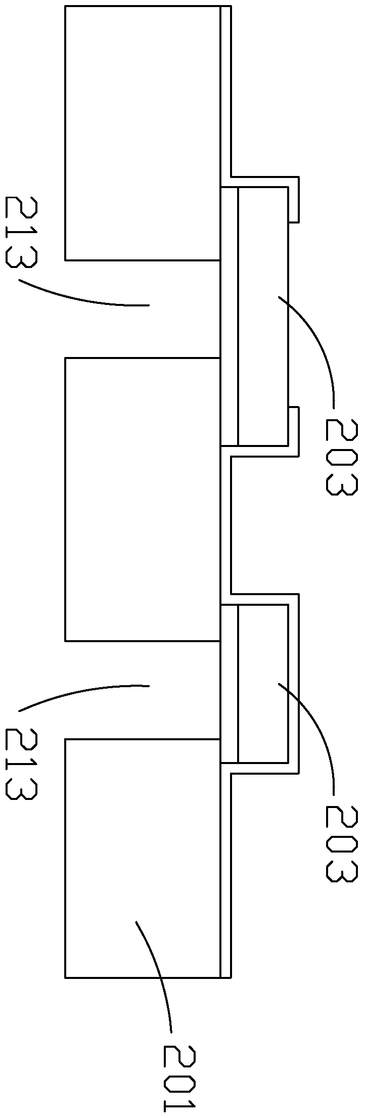
[0033] FIG. 2A is a schematic cross-sectional structure diagram of a specific embodiment of the improved structure of copper metal on the back of the semiconductor device before the back copper metallization of the present invention. It includes a substrate 201 , an active layer 203 and at least one guide hole 213 . The substrate 201 is usually made of semiconductor materials such as gallium arsenide (GaAs), indium phosphide (InP), gallium nitride (GaN) or silicon carbide (SiC). An active layer 203 is disposed on the front side of the substrate 201, and the active layer 203 includes at least one integrated circuit. Since the integrated circuit in the active layer 203 needs a grounding point, the required number of backside vias 213 will be made by etching technology on the back side of the substrate 201, through which the integrated circuit in the active layer 203 can The ground of the is connected to the ground plane of the remote configuration.

[0034]FIG. 2B is a schemat...


PUM


Abstract

An improved structure of backside copper metal for semiconductor devices, wherein the improved structure comprises sequentially from top to bottom an active layer, a substrate, a backside metal seed layer, a high-temperature sustaining buffer layer, a backside metal layer and at least one oxidation resistant layer, wherein the backside metal seed layer contains Pd and P, the high-temperature sustaining buffer layer is made of Ni, Ag or Ni alloys, and the backside metal layer is made of Cu. The semiconductor chip using the structure provided by the present invention can sustain high-temperature operations. After a persistant high temperature test, the backside metal layer structures sustain the completeness of the structure without generating gap, stripping or crack, a phenomena of imperfect earth is not easy to generate, and a characteristic of persistent high temperature operation resistance of the chip and the reliablity of the chip are effectively improved.

Description

technical field [0001] The present invention relates to an improved structure of copper metal on the back of a semiconductor element, especially a kind of copper as the back metal layer, the back metal seed layer contains palladium (Pd) and phosphorus (P), and a layer is inserted between the two layers The long-lasting high-temperature buffer layer enables the semiconductor element to have an improved structure of long-lasting high-temperature operation characteristics. Background technique [0002] The manufacturing process of the semiconductor device usually includes a backside metallization process, which is related to the flexural strength, heat dissipation and grounding characteristics of the semiconductor device. Fig. 1 is a schematic diagram of an existing copper metal structure on the back of a semiconductor element, wherein the structure sequentially includes a substrate 101, a diffusion barrier layer 105, a stress relief metal layer 107, a back metal layer 109 and ...

Claims


Application Information

Patent Timeline
Patent Type & Authority Patents(China)
IPC IPC(8): H01L23/482H01L23/485
Inventor 朱文慧花长煌陈建成
Owner WIN SEMICON
Features
  • R&D
  • Intellectual Property
  • Life Sciences
  • Materials
  • Tech Scout
  • Unparalleled Data Quality
  • Higher Quality Content
  • 60% Fewer Hallucinations
Learn More