Flexible transparent conductive film preparation method

A transparent conductive film, transparent conductive technology, applied in conductive materials dispersed in non-conductive inorganic materials, cable/conductor manufacturing, conductor/cable insulation, etc. , high cost of photolithography, to achieve the effect of good water and oxygen barrier effect, high conductivity, prolong life effect

Active Publication Date: 2017-04-26
王磊
View PDF5 Cites 21 Cited by
  • Summary
  • Abstract
  • Description
  • Claims
  • Application Information

AI Technical Summary

Problems solved by technology

Among them, the oxide solution is not suitable for flexible use; the surface roughness of the metal grid structure is relatively large, and the steps are cumbersome, and the cost of lithography is high; the light transmittance and conductivity of ultra-thin metal films cannot be achieved at the same time

Method used


Image

  • Flexible transparent conductive film preparation method
  • Flexible transparent conductive film preparation method
  • Flexible transparent conductive film preparation method

Examples


Embodiment 1

[0042] The preparation method of the flexible transparent conductive film of the present embodiment comprises the following steps:

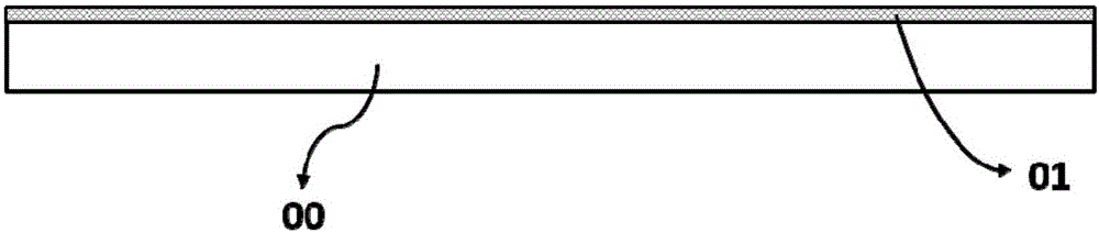
[0043] (1) On a clean glass substrate 00, first deposit a layer of SiN with a thickness of 100 nm by chemical vapor deposition (CVD) X Inorganic film as release layer 01, such as figure 1 shown;

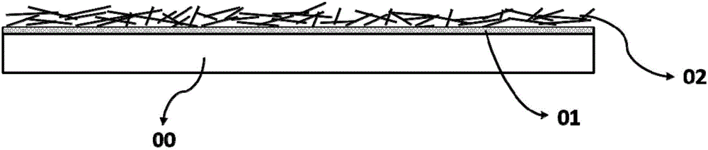
[0044] (2) Spin-coat the silver nanowire dispersion on the release layer 01 prepared in step (1) to obtain a uniform silver nanowire conductive layer 02, such as figure 2 shown;

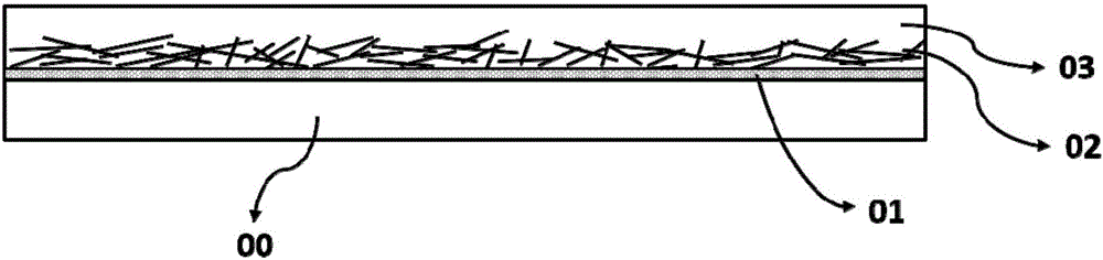
[0045] (3) On the silver nanowire conductive layer, prepare a layer of PDMS coating with a thickness of 20 μm as the polymer support layer 03 by spin coating, and leave it at room temperature for 1 hour, and then bake it in an oven at 120 ° C Roast for 1h, such as image 3 shown;

[0046] (4) Deposit a layer of Al with a thickness of 100nm on the PDMS film by atomic layer deposition (ALD) 2 o 3 The film acts as a water and oxygen barrier layer 04, such as Figure 4 sh...

Embodiment 2

[0054] The preparation method of the flexible transparent conductive film of the present embodiment comprises the following steps:

[0055] (1) On a clean glass substrate, first prepare a layer of polyimide film as a release layer by the method of slit coating;

[0056] (2) On the release layer, a layer of copper nanowire conductive layer is prepared by using a scraper coating method;

[0057] (3) Then on the copper nanowires, spin-coat a layer of CYTOP coating with a thickness of 10um as a polymer support layer, and bake in an oven at 80°C for 2h;

[0058] (4) Then use ALD on the CYTOP film to prepare a layer of Al with a thickness of 100nm 2 o 3 / MgO laminated film as water and oxygen barrier layer, in which Al 2 o 3 deposited alternately with MgO thin films, Al 2 o 3 The ratio of deposition cycles to MgO is 50 to 10;

[0059] (5) Then in Al 2 o 3 Lay a PSA lamination layer with a thickness of 50um on the film;

[0060] (6) Lay a PEN film with a thickness of 100um ...


PUM

PropertyMeasurementUnit
thicknessaaaaaaaaaa
thicknessaaaaaaaaaa
thicknessaaaaaaaaaa

Abstract

The invention discloses a flexible transparent conductive film preparation method including the steps of composite conducting layer preparation, water-oxygen barrier layer deposition, flexible substrate applying, and dissociation. The invention further discloses a flexible transparent conductive film, from the bottom to the top, successively includes a flexible substrate, an adhesive layer, a water-oxygen barrier layer, and a composite conductive layer; and the composite conductive layer comprises a transparent polymer support layer and a transparent conductive network from the bottom to the top. The method realizes the preparation of a transparent conductive film having a high conductivity and a flat surface, and the obtained flexible transparent conductive film has a bending-resistant capability.

Description

technical field [0001] The invention relates to the field of flexible electronics, in particular to a method for preparing a flexible transparent conductive film. Background technique [0002] Transparent electrode materials are required in the fields of thin-film photovoltaic cells, flat panel displays, and touch screens, and the most widely used transparent electrode material is indium tin oxide (ITO), which is composed of two oxide materials indium oxide and tin oxide. Deposited under the ratio. Under the requirement that the transmittance of visible light is greater than 90%, it can still achieve a relatively low sheet resistance (10-100Ω / □), so it has excellent electrical conductivity. However, metal indium is a scarce resource, and the global indium reserves are estimated to be only 50,000 tons. Therefore, with the continued development of the optoelectronic industry, the price of ITO will rise rapidly with the rapid mining of indium. Moreover, although ITO has excel...

Claims


Application Information

Patent Timeline
Patent Type & Authority Applications(China)
IPC IPC(8): H01B13/32H01B1/22H01B5/14B82Y30/00
CPCB82Y30/00H01B1/22H01B5/14H01B13/32
Inventor 徐苗阮崇鹏王磊李民邹建华陶洪彭俊彪许志平
Owner 王磊
Why Eureka
Try Eureka