High-voltage porcelain insulating semiconductor glaze

A technology of insulating semiconductor and high-voltage porcelain, which is applied in the field of semiconductor glaze, can solve the problems of insufficient smoothness of semiconductor glaze, rough surface of semiconductor glaze, low structural stability, etc., and achieve good suspension performance of glaze slurry, good gloss, and accelerated melting efficiency Effect

Active Publication Date: 2017-05-10
CHONGQING PIGEON ELECTRIC PORCELAIN CO LTD
View PDF6 Cites 3 Cited by
  • Summary
  • Abstract
  • Description
  • Claims
  • Application Information

AI Technical Summary

Problems solved by technology

[0005] However, this solution has the following problems: 1. The content of ferric oxide in this formula is too high, which will cause the content structure of the formed semiconducting glaze to be loose, the structural stability is not high, and the smoothness of the semiconducting glaze is not enough, relatively dull, semiconducting The surface of the glaze is relatively rough; 2. Generally, compounds containing pota

Method used


Image

  • High-voltage porcelain insulating semiconductor glaze
  • High-voltage porcelain insulating semiconductor glaze
  • High-voltage porcelain insulating semiconductor glaze

Examples


Embodiment Construction

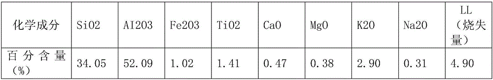
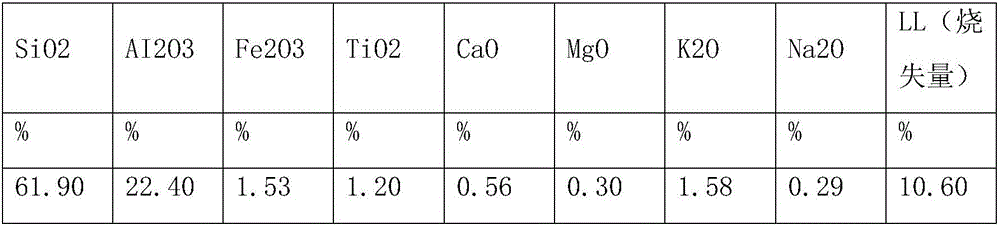
[0017] 1. Physical and chemical properties of raw materials

[0018] High-voltage ceramic insulating semiconducting glaze, made of ten kinds of raw materials including high-potassium and low-iron feldspar, quartz powder, forged talc, mud, barium carbonate, Dongsheng soil, iron oxide red, chromium oxide green, titanium dioxide and spodumene , the specific physical and chemical properties of raw materials are as follows:

[0019] 1. High-potassium and low-iron feldspar: Fujian feldspar is used, produced in Sanlian Mineral Products Processing Plant in Shaowu City, Fujian Province.

[0020] (1) Appearance quality

[0021] Before burning: yellow or light yellow powder.

[0022] After firing: It is in the shape of white frit, round and smooth, with a smooth cross-section and a small amount of black spots evenly distributed.

[0023] (2) Chemical analysis

[0024] SiO2 AI2O3 Fe2O3 TiO2 CaO MgO K2O Na2O LL % % % % % % % % % 66.2 16.0 0.2 ...


PUM


Abstract

The invention relates to the technical field of semiconductor glaze, and in particular relates to a high-voltage porcelain insulating semiconductor glaze. The semiconductor glaze is prepared from the following components in parts by weight: 25-35 parts of high-potassium and low-iron feldspar, 8-14 parts of mud, 4-10 parts of Dongsheng soil, 1-4 parts of calcined talc, 20-30 parts of quartz powder, 2-4 parts of barium carbonate, 12-18 parts of iron oxide red, 1-3 parts of chrome oxide green, 9-12 parts of titanium dioxide and 1-2 parts of spodumene. The semiconductor glaze is high in structure stability, fine in surface and glossy in surface, the eutectic point is reduced, and the melting efficiency is improved; and meanwhile, the combining capacity of the semiconductor glaze after being glazed is improved by adopting the Dongsheng soil and mud.

Description

technical field [0001] The invention relates to the technical field of semiconductor glazes, in particular to high-voltage porcelain insulating semiconductor glazes. Background technique [0002] Semiconductor glaze is a kind of glaze with special properties for high-voltage electromagnetic, and its surface resistivity is between that of insulator and conductor. Semiconductor glaze is usually formed by adding a certain amount of conductive metal oxide or compound to ordinary electric enamel. The formed microstructure is different from ordinary glazes. In addition to a large number of glass phases and a small amount of bubbles, semiconductor glazes also contain various forms of conductive crystals or solid solutions. These conductive phases run through the glass matrix to form an uninterrupted conductive network. [0003] The conductivity of semiconductor glaze mainly depends on the conductivity of the semiconductor crystal phase in the glaze. When the semiconductor crystal...

Claims


Application Information

Patent Timeline
IPC IPC(8): C03C8/20C03C1/04C04B41/86C03C8/16
CPCC03C1/04C03C8/16C03C8/20C04B41/5022C04B41/86C04B41/4535
Inventor 姚绍明薛征峰罗汉英
Owner CHONGQING PIGEON ELECTRIC PORCELAIN CO LTD
Why Eureka
Try Eureka