Silicon-based display adopting digital-analog hybrid drive

A display and silicon-based technology, applied in static indicators, instruments, etc., can solve problems such as high data bandwidth, achieve the effect of reducing area requirements, increasing pixel density, and reducing accuracy requirements

Active Publication Date: 2017-05-10
南京昀光科技有限公司
View PDF4 Cites 28 Cited by
  • Summary
  • Abstract
  • Description
  • Claims
  • Application Information

AI Technical Summary

Problems solved by technology

However, under the conditions of high resolution and high refresh rate, the digital scanning strategy requires extremely high data bandwidth, which poses higher challenges to system performance

Method used


Image

  • Silicon-based display adopting digital-analog hybrid drive
  • Silicon-based display adopting digital-analog hybrid drive
  • Silicon-based display adopting digital-analog hybrid drive

Examples


Embodiment 1

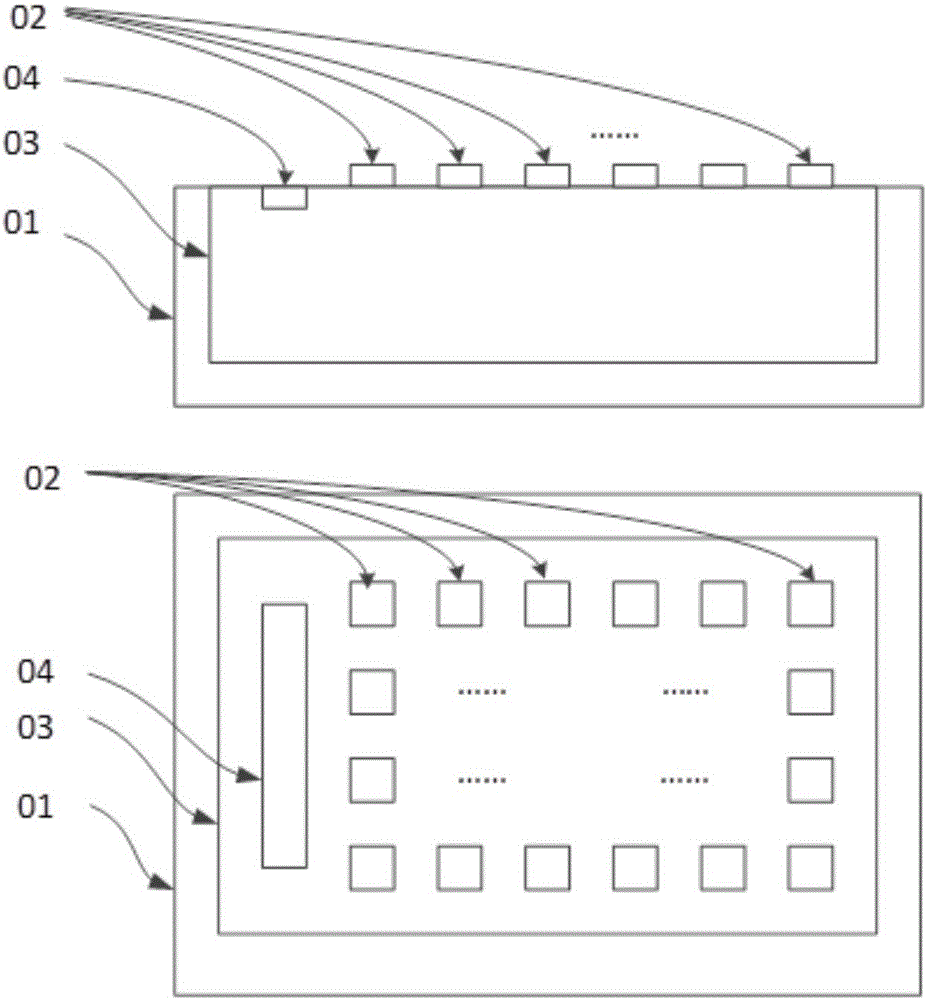
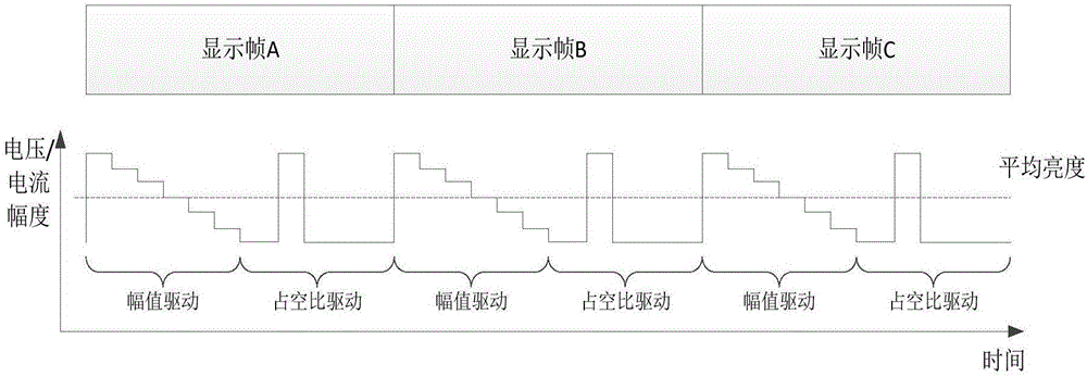
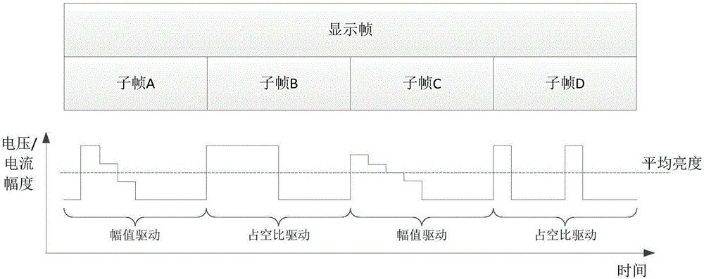
[0047] figure 1 The basic structure of a silicon-based microdisplay adopted in the present invention is illustrated, the upper part is a side view, and the lower part is a top view, which at least includes a semiconductor silicon substrate 01 and a pixel 02 on the surface of the silicon substrate and a driving circuit 03 contained in the silicon substrate and Interface 04, the drive circuit 03 at least includes a metal-oxide semiconductor field effect transistor and at least two metal layers; the brightness of the pixel 02 in a specific display frame is determined by the output current or voltage of the pixel in the display frame The amplitude of the pixel and the time duty cycle of the output current or voltage of the pixel in the display frame are jointly determined; the display frame includes the pixel grayscale information in a specific display area through the interface 04 through the drive circuit 03 is the process of transmitting to the pixel 02; the specific display fr...

Embodiment 2

[0052] This embodiment is basically the same as Embodiment 1, especially in that:

[0053] The pixel 02 emits light actively through the luminescent substance 05 on the surface of the pixel or reflects the light source through the reflective substance 06 on the surface of the pixel to form light. Phenomenon substances include organic electroluminescence devices or light-emitting diode devices; the reflective substance 06 is a substance that reflects or transmits light by applying current or voltage, including liquid crystals. The relationship between the luminescent substance 05 and the silicon-based microdisplay is as follows Figure 4 As shown, the relationship between the reflective material 06 and the silicon-based microdisplay is as follows Figure 5 shown.

Embodiment 3

[0055] This embodiment is basically the same as Embodiment 1, especially in that:

[0056] The driving circuit 03 includes a pixel unit circuit 10, the pixel unit circuit 10 at least includes an output transistor 20 and a pixel electrode 08, the output transistor 20 outputs current or voltage to the pixel electrode 08 through a conductive via 07, and the pixel electrode 08 is the anode or cathode of pixel 02. The relationship between the pixel unit circuit 10 and the silicon-based microdisplay is as follows Image 6 shown.


PUM


Abstract

The invention discloses a silicon-based display adopting digital-analog hybrid drive. Pixels are driven to emit light through the method of combining the simulation amplitude modulation drive strategy and a digital pulse width modulation drive strategy, wherein the luminance of the pixels is determined by output current or voltage amplitude of the pixels in the subframe and the duty ratio of time of the output current or voltage of the pixels in the subframe, the frame of image is divided into a plurality of different digital subframes and simulation subframes, the digital drive strategy is adopted for the digital subframes, the time proportionable drive mode or luminance proportionable drive mode is adopted, the simulation drive strategy is adopted for the simulation subframes, many digital-analog converters with few digits are adopted, input data is converted into amplitude quantity of voltage or current, so that the pixels emit light, and the simulation subframes and the digital subframes are combined to generate the final display frame. The requirements of the simulation amplitude modulation drive strategy for the digital-analog converter and the requirements of the pixel circuit for the precision of analog quantity are reduced, and the conversion speed of the digital-analog converter and the contrast of the pixel luminance are improved.

Description

technical field [0001] The invention relates to the technical field of microelectronics and flat panel display, in particular to a digital-analog fusion-driven silicon-based display. Background technique [0002] A silicon-based microdisplay is a microdisplay based on a silicon semiconductor integrated circuit, and the driver circuit of the display is integrated in the silicon substrate. According to different display principles, silicon-based microdisplays can be divided into silicon-based organic light-emitting microdisplays, silicon-based light-emitting diode microdisplays, silicon-based liquid crystal microdisplays, and silicon-based micromechanical microdisplays. The pixels of silicon-based microdisplays are very small, and it produces a large-screen display effect through an optical system, which can be applied to military, industrial, medical and consumer electronics. At present, silicon-based microdisplays are developing toward higher resolution, higher grayscale le...

Claims


Application Information

Patent Timeline
Patent Type & Authority Applications(China)
IPC IPC(8): G09G3/36G09G3/3225G09G3/32
CPCG09G3/32G09G3/3225G09G3/3648
Inventor 季渊穆廷洲褚勇男余云森沈伟星
Owner 南京昀光科技有限公司
Why Eureka
Try Eureka