Manufacture method for twin pole device resisting low dosage rate irradiation

A bipolar device, low dose rate technology, applied in semiconductor/solid-state device manufacturing, semiconductor devices, electrical components, etc. With radiation resistance and other issues, to achieve the effect of reducing the total number of defects, small stress and high reliability

Active Publication Date: 2017-05-10
BEIJING MXTRONICS CORP +1
View PDF2 Cites 7 Cited by
  • Summary
  • Abstract
  • Description
  • Claims
  • Application Information

AI Technical Summary

Problems solved by technology

Although the traditional method has simple process steps and short tape-out cycle, its disadvantages are: (1) SiO as the electrode isolation dielectric layer 2 Direct contact with the base of the device is a key part that affects the ability of the device to withstand low dose rate radiation
Although Si 3 N 4 It has a strong resistance to external water vapor and movable charges, but Si 3 N 4 It cannot fix the mobile charge induced in the oxide layer during irradiation, which determines the traditional Si 3 N 4 The passivation film of the material does not have the ability to resist radiation

Method used


Image

  • Manufacture method for twin pole device resisting low dosage rate irradiation
  • Manufacture method for twin pole device resisting low dosage rate irradiation
  • Manufacture method for twin pole device resisting low dosage rate irradiation

Examples


Embodiment

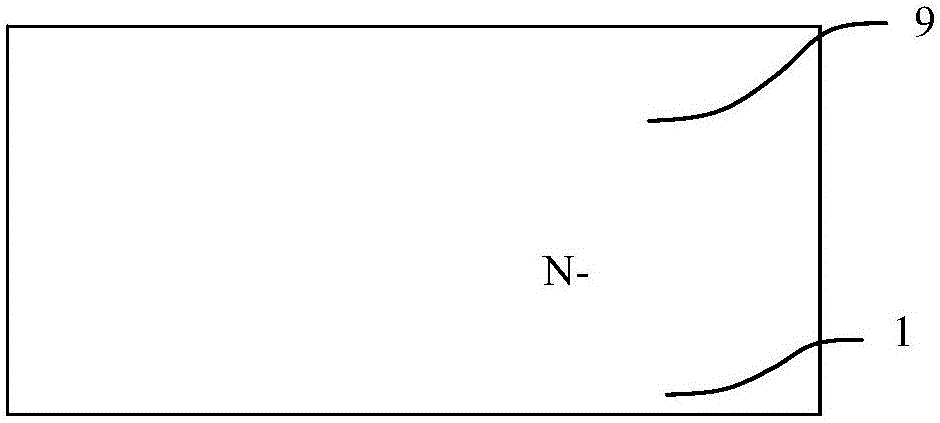
[0057] (1) Material selection: such as figure 2 , select the N-type silicon epitaxial wafer 1 with crystal orientation as the substrate material, the total thickness of the silicon wafer is 525μm, the N-type epitaxial thickness is 50um, and the doping concentration is 2e14cm -3 .

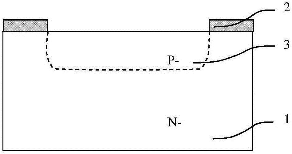
[0058] (2) Base manufacturing: such as image 3 , using silicon N-type epitaxial wafer 1 as the base material, depositing Oxide layer 2. Then perform photolithography on the base of the triode, and then use a wet etching process to expose the injection window in the base area, with a dose of 1e14cm -2 Boron implantation in the base area, and then oxidize the boron-injected N-type epitaxial wafer at a temperature of 1200°C for 100 minutes. forming a P-type transistor base region 3 on the polished surface of the N-type epitaxial wafer;

[0059] (3) Concentrated boron contact: such as Figure 4 , in the area of ​​the base region 3 of the triode, photolithography concentrated boron pattern, ...


PUM


Abstract

The invention discloses a manufacture method for a twin pole device resisting low dosage rate irradiation. According to the invention, a multi-layer passivation structure employing PSG (Phosphorosilicate Glass) + SiO2 double-layer electrode isolation medium and SiO2+BPSG (Boron Phosphorosilicate Glass)+SiO2. By adopting the above structure, total number of defects in the electrode isolation medium layer is reduced substantially on one hand. On the other hand, through adsorption of positive charges of the PSG and the BPSG, accumulation of the positive changes generated in the irradiation environment on the surface of Si-SiO2 is prevented and further the low dosage rate irradiation resistance of the twin-pole device is improved. The manufacture method provided by the invention is simple in technical procedure and is compatible to Si manufacture technique that is widely applied currently, and can be used for manufacturing the twin pole device having low dosage rate irradiation resistance.

Description

technical field [0001] The invention relates to a method for manufacturing a bipolar device resistant to low dose rate radiation. The bipolar device has a double-layer electrode isolation medium and a multi-layer passivation structure, and belongs to the field of design and manufacture of radiation-resistant semiconductor devices. Background technique [0002] Bipolar devices have the advantages of good current drive capability, high linearity, low noise, and good matching characteristics. They are often used as switches and signal amplifiers, and are widely used in space electronic equipment. [0003] Bipolar devices operating in space will be subject to various radiations such as charged particles on the earth and solar cosmic rays, and the performance of the devices will be greatly damaged. Radiation will be in the Si-SiO of the bipolar device 2 The interface causes the accumulation of positive charges and introduces the interface state, which increases the surface poten...

Claims


Application Information

Patent Timeline
Patent Type & Authority Applications(China)
IPC IPC(8): H01L21/331H01L29/40H01L29/423
Inventor 赵昕王传敏杨小兵殷丽孙金池郝贵争
Owner BEIJING MXTRONICS CORP
Why Eureka
Try Eureka