Carbon quantum dot enhanced photoelectric detector and preparation method thereof
A technology of photodetectors and carbon quantum dots, applied in the field of photodetectors, can solve problems that have not been found and reported, and achieve the effects of simple preparation process, easy promotion and low cost
- Summary
- Abstract
- Description
- Claims
- Application Information
AI Technical Summary
Problems solved by technology
Method used
Image
Examples
Embodiment 1
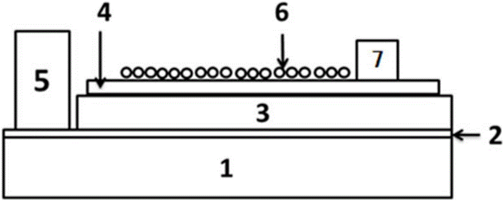
[0022] 1) Clean the polyimide flexible substrate in deionized water and dry it;
[0023] 2) Using magnetron sputtering to deposit 40 nanometers of indium-doped germanium on a polyimide flexible substrate;
[0024] 3) Depositing a 6-micron-thick germanium tin layer on the indium-doped germanium tin layer by physical vapor deposition technology, and reserving an area for growing the first electrode on the ITO layer;
[0025] 4) Depositing germanium silicide on the germanium tin layer;
[0026] 5) spin coating the carbon quantum dot solution on the germanium silicide, and reserve an area for growing the second electrode on the germanium silicide; the diameter of the carbon quantum dot is 1nm-1μm;
[0027] 6) Coating silver paste on the reserved area of germanium silicide and the reserved area on the ITO layer and drying; obtaining a germanium silicide / germanium tin oxide photodetector enhanced by carbon quantum dots.
Embodiment 2
[0029] 1) Clean the glass substrate in deionized water and dry it;
[0030] 2) Deposit 200 nanometer thick fluorine-doped germanium tin oxide on the glass substrate by magnetron sputtering;
[0031] 3) Depositing an 8 micron-thick germanium tin layer on the fluorine-doped germanium tin layer by physical vapor deposition technology, and reserving an area for growing the first electrode on the FTO layer;
[0032] 4) Depositing germanium silicide on the germanium tin layer;
[0033] 5) Spraying a carbon quantum dot solution on the germanium silicide, and reserving an area for growing the second electrode on the germanium silicide layer; the diameter of the carbon quantum dot is 1nm-1μm;
[0034] 6) thermally evaporating gold electrodes at the reserved area of the germanium silicide layer and the reserved area on the fluorine-doped germanium tin oxide layer; obtaining a germanium silicon oxide / germanium tin oxide photodetector enhanced by carbon quantum dots.
Embodiment 3
[0036] 1) Clean the ceramic substrate in deionized water and dry it;
[0037] 2) Electron beam evaporation is used to deposit nickel metal with a thickness of 60 nanometers on the ceramic substrate;
[0038] 3) Depositing a germanium tin oxide layer with a thickness of 5 microns on the nickel metal layer by chemical water bath method, and reserving an area for growing the first electrode on the nickel metal layer;
[0039] 4) Depositing germanium silicide on the germanium tin layer;
[0040] 5) preparing a carbon quantum dot film on the germanium silicide layer, and reserving an area for growing the second electrode on the germanium silicide layer;
[0041] 6) screen-print silver electrodes on the reserved area of the germanium silicide layer and the reserved area on the nickel metal layer; obtain a germanium silicide / germanium tin oxide photodetector enhanced by carbon quantum dots.
PUM
| Property | Measurement | Unit |
|---|---|---|
| diameter | aaaaa | aaaaa |
Abstract
Description
Claims
Application Information
