A surface plasmon electric excitation and electrical modulation integrated device and its manufacturing method

A surface plasmon, electro-excitation technology, applied in electrical components, semiconductor devices, circuits, etc., can solve problems such as limited application range, surface plasmon modulation without electro-excitation, and inability to integrate devices , to achieve the effect of simple process and easy integration

Active Publication Date: 2018-08-10
TECHNICAL INST OF PHYSICS & CHEMISTRY - CHINESE ACAD OF SCI
View PDF7 Cites 0 Cited by
  • Summary
  • Abstract
  • Description
  • Claims
  • Application Information

AI Technical Summary

Problems solved by technology

However, the disadvantage of this scheme is that it can only be used for optically excited metal structure plasmon resonance peak modulation, and device integration cannot be performed; it can only be applied to the mid-infrared band, which limits the scope of application.
[0010] The above-mentioned surface plasmon modulation scheme using materials such as barium titanate, Si, and graphene only modulates the optically excited surface plasmons, but does not modulate the electrically excited surface plasmons.

Method used


Image

  • A surface plasmon electric excitation and electrical modulation integrated device and its manufacturing method
  • A surface plasmon electric excitation and electrical modulation integrated device and its manufacturing method
  • A surface plasmon electric excitation and electrical modulation integrated device and its manufacturing method

Examples


Embodiment 1

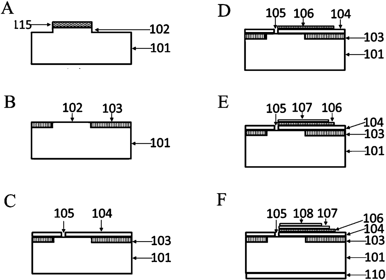
[0056] Taking an indium phosphide (InP)-based quantum well material with a wavelength of λ≈1.55 μm as an example, the structure and manufacturing process of the surface plasmon electric excitation and electrical modulation integrated device of the present invention will be described with reference to the accompanying drawings.

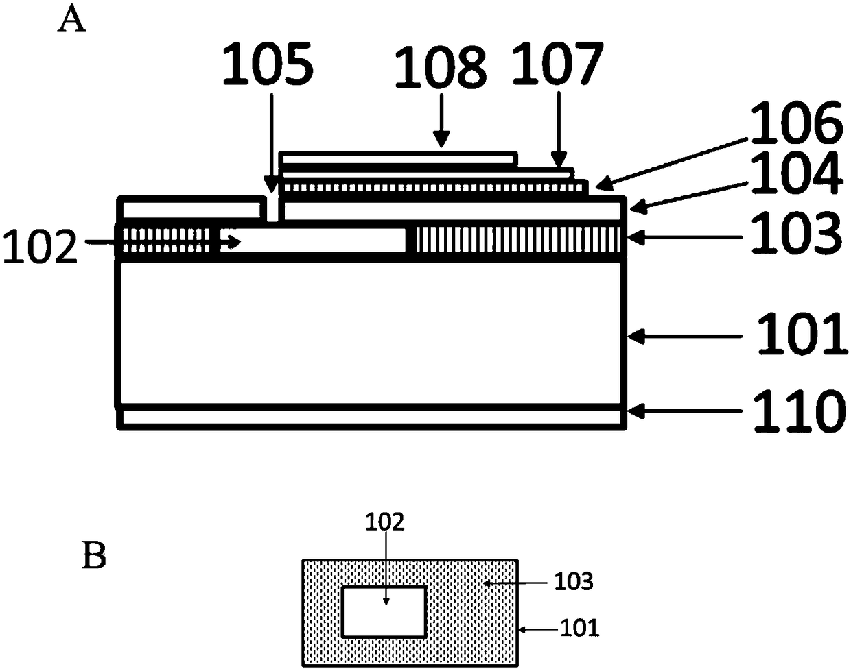
[0057] figure 1 A is a schematic diagram of the structure of the surface plasmon electric excitation and electrical modulation integrated device. Including a semiconductor substrate 101, a semiconductor active structure 102 formed on the semiconductor substrate 101, a first dielectric layer 103 formed around the semiconductor active structure 102 (such as figure 1 Shown in B), the metal electrode and the waveguide structure 104 formed on the semiconductor active structure 102 and the first dielectric layer 103 are formed with the directional coupling structure 105, the second dielectric layer 106 formed on the metal electrode and the waveguide structur...

Embodiment 2

[0069] A surface plasmon electric excitation and electrical modulation integrated device and its manufacturing method, repeating Example 1, the difference is:

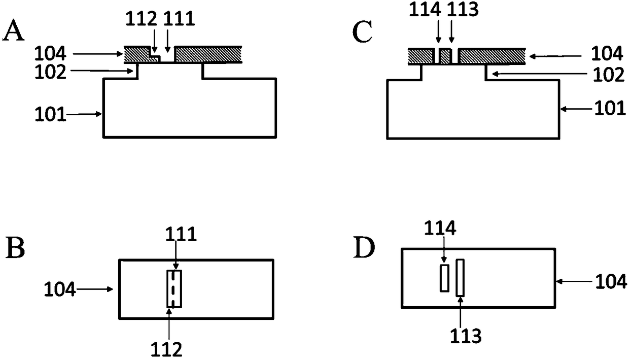
[0070] The thickness of the metal electrodes and waveguide structure 104 is 150-250 nm. The directional coupling structure 105 is composed of asymmetric grooves 113 and 114, such as image 3 C and image 3 As shown in D, the length of the groove 113 is about 200-500nm and the width is about 80-150nm; the length of the groove 114 is 500-1000nm and the width is 80-150nm, and the distance between the centers of the grooves 113 and 114 is 200-400nm. The thickness of the groove 113 and the groove 114 in the directional coupling-out structure 105 does not exceed the thickness of the metal electrode and the waveguide structure 104 .

[0071] The second dielectric layer 106 adopts the material grown by atomic layer deposition-aluminum oxide (Al 2 o 3 ), the growth temperature is 100-140°C, the thickness is 40-80nm, the sur...


PUM

PropertyMeasurementUnit
thicknessaaaaaaaaaa
thicknessaaaaaaaaaa
thicknessaaaaaaaaaa

Abstract

A surface plasmon electro-excitation and electrical modulation integrated device comprises a back electrode, a semiconductor substrate, a semiconductor active structure, a first dielectric layer, a metal electrode and waveguide structure, a directional coupling structure, a second dielectric layer, a graphene structure, and a graphene metal electrode and waveguide structure. By electrically injecting a semiconductor quantum well material, the surface plasmons on metal and semiconductor medium interfaces are excited by means of near-field coupling and are propagated on a metal-medium waveguide after directional coupled output, and thus, surface plasmon electro-excitation is realized. Based on the fact that the Fermi level and dielectric constant change when the concentration of graphene carriers changes with change of gate voltage applied, the transmission bandwidth and high speed of electro-excited surface plasmons are modulated through the voltage applied to graphene in a field effect transistor-resembling structure composed of metal electrodes, a second dielectric layer and graphene.

Description

technical field [0001] The invention relates to a micro-nano optoelectronic integrated device and a manufacturing method thereof. More specifically, it relates to a surface plasmon electric excitation and electrical modulation integrated device and a manufacturing method thereof. Background technique [0002] Integrated electronic devices are one of the basic functional units of traditional information technology, but restricted by nanometer size, as predicted by Moore's law, the development of integrated electronic devices is gradually approaching its physical limit. Photon integrated circuits and optical computing use photons with fast propagation speed and large transmission capacity as information carriers, which has huge advantages. Surface plasmons based on metal nanostructures can break through the limitations of the traditional optical diffraction limit and light field confinement capabilities, and can manipulate photons at the nanoscale; therefore, plasmonic integr...

Claims


Application Information

Patent Timeline
Patent Type & Authority Patents(China)
IPC IPC(8): H01L33/00H01L33/06
CPCH01L33/0041H01L33/06
Inventor 李敬孟祥敏田利丰夏静
Owner TECHNICAL INST OF PHYSICS & CHEMISTRY - CHINESE ACAD OF SCI
Why Eureka
Try Eureka