A Monolithically Integrated Tunnel Junction Laser for Microwave Oscillating Source

A microwave oscillation source and monolithic integration technology, which is applied in lasers, laser components, semiconductor lasers, etc., can solve the problems of low modulation rate of microwave oscillation source, low modulation rate, and high power loss, so as to reduce phase noise and realize modulation , The effect of reducing power loss

Active Publication Date: 2020-05-19
INST OF SEMICONDUCTORS - CHINESE ACAD OF SCI
View PDF5 Cites 0 Cited by
  • Summary
  • Abstract
  • Description
  • Claims
  • Application Information

AI Technical Summary

Problems solved by technology

However, the modulation rate of the microwave oscillator source mixed and integrated by two separate devices is low, and the highest reported RF signal frequency is 1.4GHz
Therefore, the current microwave oscillation source has the problems of low modulation rate, high phase noise, high power loss, and complex structure.

Method used


Image

  • A Monolithically Integrated Tunnel Junction Laser for Microwave Oscillating Source
  • A Monolithically Integrated Tunnel Junction Laser for Microwave Oscillating Source
  • A Monolithically Integrated Tunnel Junction Laser for Microwave Oscillating Source

Examples


Embodiment 1

[0041] Embodiment 1 is a monolithically integrated tunnel junction laser for a microwave oscillation source with a lasing wavelength around 1.55 μm.

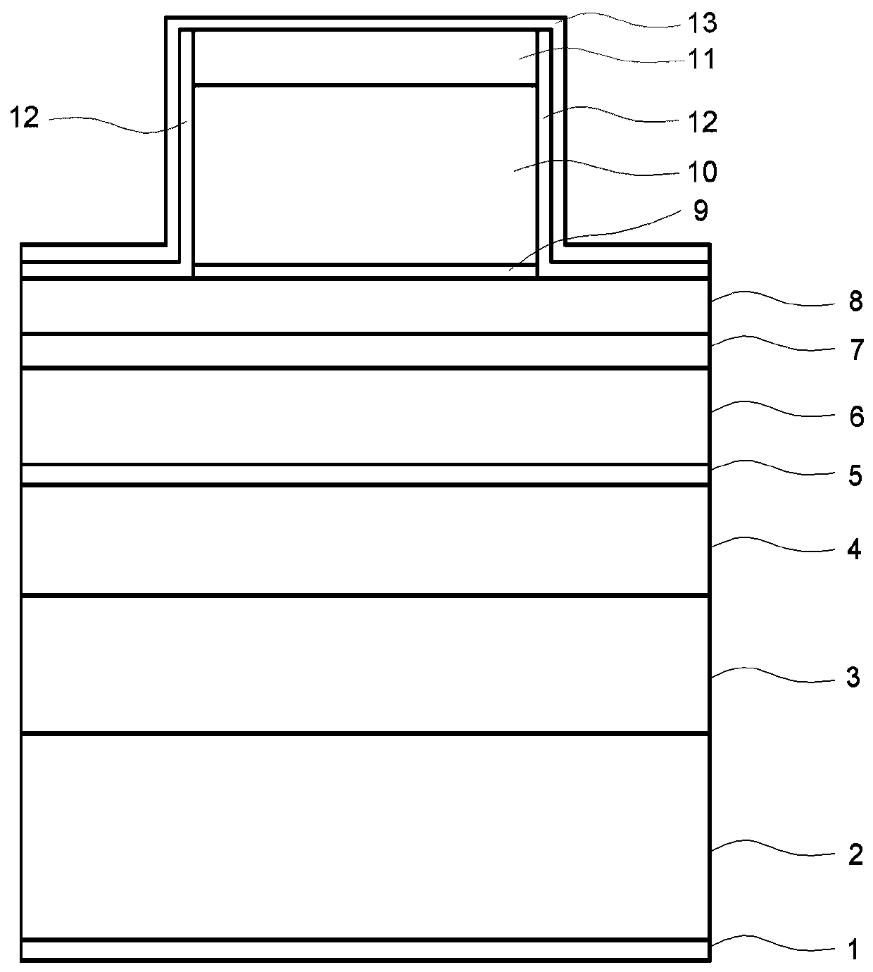
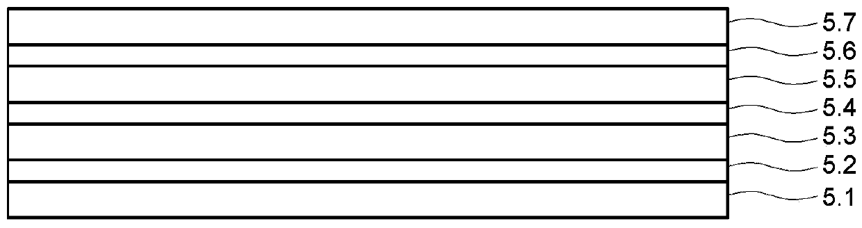
[0042] like figure 1 As shown, the monolithic integrated tunnel junction laser for microwave oscillation source in Example 1 is, from bottom to top, an N electrode 1, an N-type InP substrate 2, an N-type InP buffer layer 3, a lower confinement layer 4, a quantum Well active region 5 , upper confinement layer 6 , grating layer 7 , N-type InP layer 8 , tunnel junction 9 , P-type InP capping layer 10 , P-type contact layer 11 , insulating isolation layer 12 and P electrode 13 .

[0043] N electrode 1, N-type InP substrate 2, N-type InP buffer layer 3, lower confinement layer 4, quantum well active region 5, upper confinement layer 6, grating layer 7, N-type InP layer 8 have the same width; On the type InP layer 8 is a ridge waveguide structure formed by a tunnel junction 9, a P type InP cap layer 10 and a P type contact layer 11. ...

Embodiment 2

[0056] Embodiment 2 is a monolithically integrated tunnel junction laser for a microwave oscillation source with a lasing wavelength around 1.31 μm.

[0057] like figure 1 As shown, the monolithic integrated tunnel junction laser used for the microwave oscillation source in Example 2 is, from bottom to top, an N electrode 1, an N-type InP substrate 2, an N-type InP buffer layer 3, a lower confinement layer 4, a quantum Well active region 5 , upper confinement layer 6 , grating layer 7 , N-type InP layer 8 , tunnel junction 9 , P-type InP capping layer 10 , P-type contact layer 11 , insulating isolation layer 12 and P electrode 13 .

[0058] N electrode 1, N-type InP substrate 2, N-type InP buffer layer 3, lower confinement layer 4, quantum well active region 5, upper confinement layer 6, grating layer 7, N-type InP layer 8 have the same width; On the type InP layer 8 is a ridge waveguide structure formed by a tunnel junction 9, a P type InP cap layer 10 and a P type contact l...


PUM

PropertyMeasurementUnit
thicknessaaaaaaaaaa
thicknessaaaaaaaaaa
wavelengthaaaaaaaaaa

Abstract

The invention discloses a single-chip integrated tunnel junction laser for a microwave oscillation source, and relates to the technical field of semiconductor optoelectronic devices. The single-chip integrated tunnel junction laser for the microwave oscillation source mainly comprises an N electrode, an N-type InP substrate, an N-type InP buffer layer, a lower limiting layer, a quantum well activeregion, an upper limiting layer, a grating layer, an N-type InP layer, a tunnel junction, a P-type InP cover layer, a P-type contact layer and a P electrode. By means of the differential negative resistance characteristic of a tunnel junction during forward deviation, oscillation modulation is carried out in the device, so that the laser can directly transmit the light-borne microwaves. The phasenoise is reduced, the power loss is minimized, the structure of the device is simplified, and meanwhile high-speed modulation is realized.

Description

technical field [0001] The invention relates to the technical field of semiconductor optoelectronic devices, in particular to a monolithic integrated tunnel junction laser used for a microwave oscillation source. Background technique [0002] Microwave signals are widely used in electronic measurement, clock extraction, civil communication, electronic countermeasures, radar, etc. In traditional microwave signal generation methods, dielectric oscillators are unsatisfactory in terms of high-purity spectrum, low phase noise, and tunability. Optoelectronic oscillators (OEO) use optoelectronic feedback loop technology to obtain highly stable and low-noise microwave signals, and have become a new type of high-quality microwave signal source. [0003] OEO can generate radio frequency (Radio Frequency, RF) signals in the optical domain, and has some advantages over traditional electric oscillators, such as the signal can be propagated in the optical fiber, and signal processing can...

Claims


Application Information

Patent Timeline
Patent Type & Authority Patents(China)
IPC IPC(8): H01S5/32H01S5/22H01S5/34H01S5/343
CPCH01S5/22H01S5/32H01S5/34H01S5/34373
Inventor 李亚节周旭亮王鹏飞王梦琦于红艳李召松李稚博潘教青
Owner INST OF SEMICONDUCTORS - CHINESE ACAD OF SCI
Why Eureka
Try Eureka