Gallium nitride device schottky contact system with composite metal barrier layer
A technology of Schottky contact and composite metal layer, which is applied in the direction of semiconductor devices, electrical components, circuits, etc., can solve the problems of unfavorable manufacturing of high-reliability AlGaN/GaN HEMT devices, reduce the gate resistance of devices, and hidden dangers of reliability, etc. Expansion coefficient, small thermal conductivity, and the effect of improving work reliability
- Summary
- Abstract
- Description
- Claims
- Application Information
AI Technical Summary
Problems solved by technology
Method used
Image
Examples
Embodiment 1
[0030] Example 1. After the above-mentioned source electrode 34 and drain electrode 35 are completed, as Figure 3C A layer of dielectric layer 36 is deposited as shown, and the dielectric layer 36 covers the source and source electrodes 34 and drain electrodes 35 and the AlGaN barrier layer 33 at the same time. The materials that can be used for the dielectric layer 36 include silicon nitride (SiN) and silicon oxide (SiO 2 ), the deposition method of the dielectric layer 36 includes sputtering, electron beam evaporation, plasma enhanced chemical vapor deposition (PECVD), and the preferred dielectric material and deposition method are SiN and PECVD.
[0031] Next, if Figure 3D As shown, a window 37 called a gate foot is formed on the dielectric layer 36 between the source electrode 34 and the drain electrode 35. The formation of the gate foot window 37 generally requires steps such as coating a photoresist layer, exposure, and development on the gate. Form a window in the p...
Embodiment 2
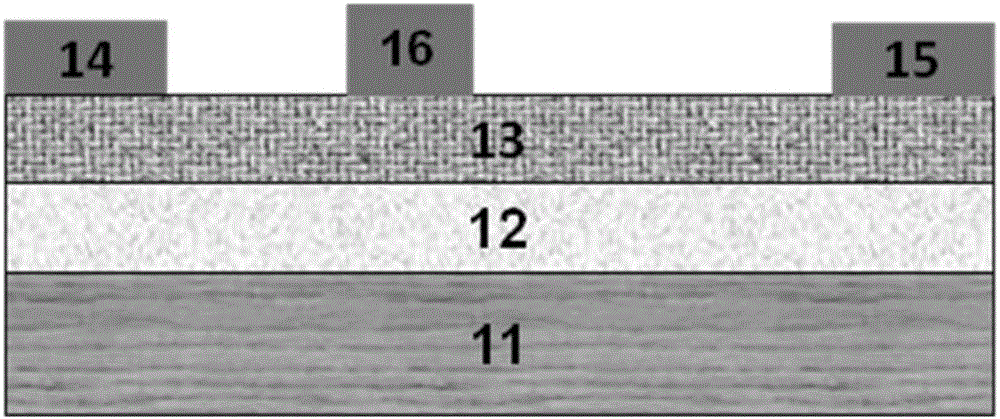
[0033] Example 2. Figures 4A-4B It is the specific implementation steps of Embodiment 2 of the present invention. Such as Figure 4A As shown, it includes a substrate 11, a GaN buffer layer 12, and an AlGaN barrier layer 13; after the source electrode 34 and the drain electrode 35 are completed, a photoresist layer 46 is applied, and is formed in the resist layer 46 through processes such as exposure and development. There is a "T"-shaped groove 47. In order to obtain the "T"-shaped groove 47, the photoresist layer 46 generally needs to be composed of two different photoresist layers, and after at least two exposures, one or two developments Obtain, for how to obtain " T " type groove 47 can refer to or deposit gate electrode metal layer on the groove 47 and photoresist layer 46 and peel off and remove photoresist layer and the gate electrode metal layer on it, thereby obtain Such as Figure 4B The gate electrode 48 is shown.
[0034] The purpose of the gate electrode 48 ...
PUM
| Property | Measurement | Unit |
|---|---|---|
| Thickness | aaaaa | aaaaa |
| Thickness | aaaaa | aaaaa |
| Thickness | aaaaa | aaaaa |
Abstract
Description
Claims
Application Information


