
Device and method for processing semiconductor material through backward multifocal lasers and electrochemistry in combined manner

A composite processing and semiconductor technology, applied in laser welding equipment, metal processing equipment, manufacturing tools, etc., can solve problems such as uneven distribution of porosity, increased control distance between light source and sample, and inability to guarantee light intensity. Good precision, avoid the taper of the hole wall, and improve the processing speed.

Inactive Publication Date: 2017-05-31
JIANGSU UNIV
View PDF9 Cites 18 Cited by
  • Summary
  • Abstract
  • Description
  • Claims
  • Application Information

AI Technical Summary

Problems solved by technology

[0008] 3. If the control distance between the light source and the sample becomes larger, the light intensity cannot be guaranteed
The appearance of large pores cannot be avoided, and as the depth of the pores increases, the distribution of porosity in the longitudinal direction is uneven

Method used


Image

  • Device and method for processing semiconductor material through backward multifocal lasers and electrochemistry in combined manner
  • Device and method for processing semiconductor material through backward multifocal lasers and electrochemistry in combined manner
  • Device and method for processing semiconductor material through backward multifocal lasers and electrochemistry in combined manner

Examples


Embodiment Construction

[0035] The present invention will be further described below in conjunction with the accompanying drawings and specific embodiments, but the protection scope of the present invention is not limited thereto.

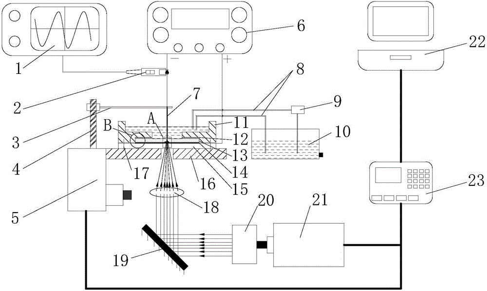
[0036] Such as figure 1 The shown laser multi-focus and electrochemical compound processing device for semiconductor materials mainly includes a multi-focus laser irradiation system, an electrochemical reaction system, an electrolyte circulation system and a motion control system.

[0037] Described motion control system mainly comprises computer 22, control cabinet 23, numerical control platform 5, and computer 22 links to each other with control cabinet 23, and control cabinet 23 links to each other with numerical control platform 5, and control cabinet 5 links to each other with pulsed laser 21, and computer 22 connects to each other through control cabinet 23. Control the movement of the numerical control platform 5 . A through hole is provided at the center of the e...


PUM

PropertyMeasurementUnit
Wavelengthaaaaaaaaaa
Pulse widthaaaaaaaaaa
Thicknessaaaaaaaaaa

Abstract

The invention provides a device and method for processing a semiconductor material through backward multifocal lasers and electrochemistry in a combined manner. The energy, frequency and wavelength of the lasers are regulated, and a multifocal laser beam acts on the back face of a semiconductor sample; on one hand, when the lasers radiate the back face of the semiconductor sample, a large amount of light can be stimulated in the semiconductor sample to generate holes, the holes move to the position of the surface of the polished semiconductor sample to participate in the electrochemistry reaction, and material corrosion removal is achieved; and on the other hand, on the back face of the semiconductor sample, the multifocal lasers gradually conduct processing inwards. A work electrode is a cathode, the semiconductor sample is used as an anode, and when the potential between the two electrodes is high, spark discharge processing is conducted; and when the potential is low, electrochemistry erosion removal is conducted. The multifocal lasers and electrochemistry act on the semiconductor sample in the combined manner, the corrosion efficiency is improved, and the surface quality of through holes is improved. When the high-precision micro-through-holes are processed in the semiconductor material, the combination effect is good in action effect, and the device and the method are suitable for precise processing.

Description

technical field [0001] The invention relates to a compound precision machining method in the field of micromachining, in particular to a device and method for back-facing multi-focus laser and electrochemical compound machining of semiconductor materials. Background technique [0002] For the current research on semiconductor material processing technology and its application, semiconductor materials represented by silicon have the characteristics of high brittleness, relatively close fracture strength and yield strength. In traditional processing at room temperature, semiconductor materials often produce cracks before plastic deformation, and it is difficult to obtain high-quality processed surfaces, so precision processing technology is particularly important. The use of composite processing technology to manufacture complex micro-systems that integrate optical, electromechanical, electromagnetic and other functions to complete certain functions has attracted worldwide att...

Claims


Application Information

Patent Timeline
IPC IPC(8): B23K26/00B23K26/402B23K26/067B23K26/08B23P23/02
CPCB23K26/0093B23K26/067B23K26/08B23K26/402B23P23/02
Inventor 张朝阳徐金磊杨敬博戴学仁顾秦铭蒋雯曹增辉
Owner JIANGSU UNIV
Learn More