Double-layer heterostructure mold, its manufacturing method and application in micro nano material preparation
A double-layer heterogeneous, manufacturing method technology, applied in the direction of nanostructure manufacturing, nanotechnology, nanotechnology, etc., can solve the problems of difficult mass production and complex preparation, and achieve easy mass production, simple preparation, high precision effect
- Summary
- Abstract
- Description
- Claims
- Application Information
AI Technical Summary
Problems solved by technology
Method used
Image
Examples
Embodiment 1
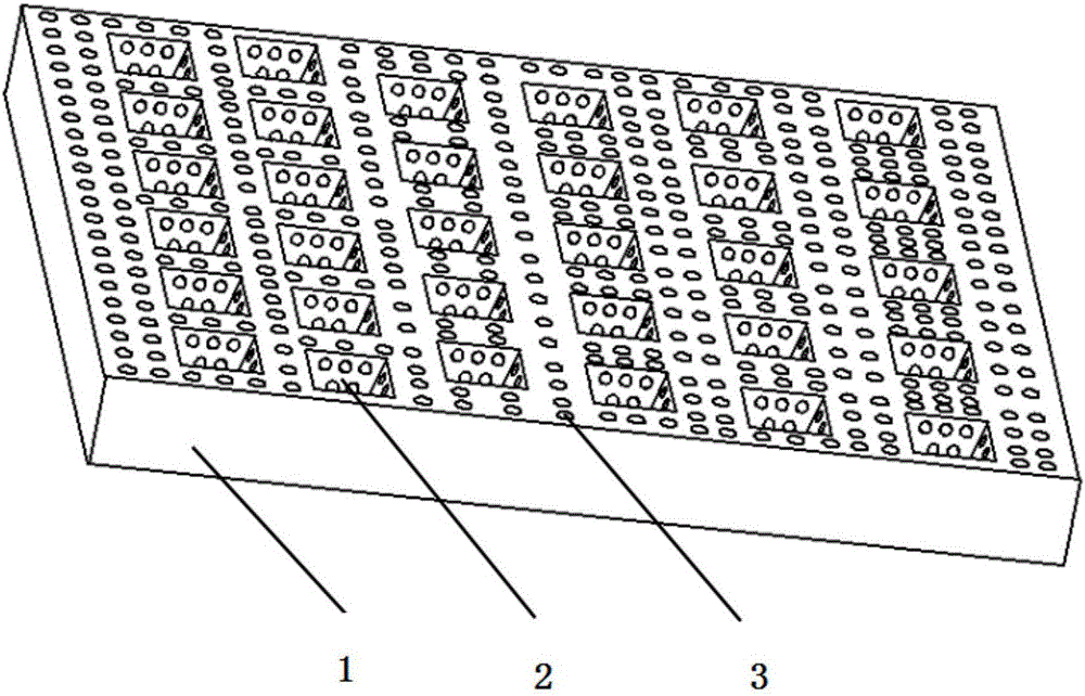
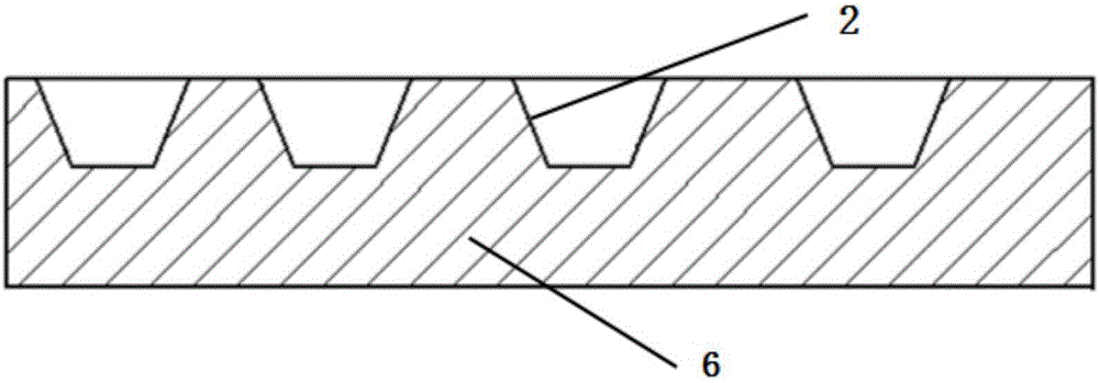
[0043] Embodiment 1 The micro-nano secondary structure mold according to the present invention includes a silicon liner 1, the upper surface of the silicon liner 1 is distributed with multiple rows of micron-scale groove groups along the axial direction of the silicon liner, and each column contains The above-mentioned groove group includes several micron-sized grooves 2 arranged equidistantly, and the axial spacing gradient of two adjacent rows of groove groups gradually increases; The groove 2 and the nanoscale pores 3 distributed on the surface of the micrometer groove 2 form a secondary structure.
[0044] The micro-groove 2 is a concave inverted quadrangular truss.
[0045]The side length of the inverted quadrangular prism of the micron groove 2 is 100 microns.
[0046] The nanoscale hole 3 is a concave hemispherical structure.
[0047] The hemispherical diameter of the nanoscale hole 3 is 200 nanometers.
Embodiment 2
[0049] According to the manufacturing method of the micro-nano secondary structure mold described in embodiment 1, the manufacturing method comprises the following steps:
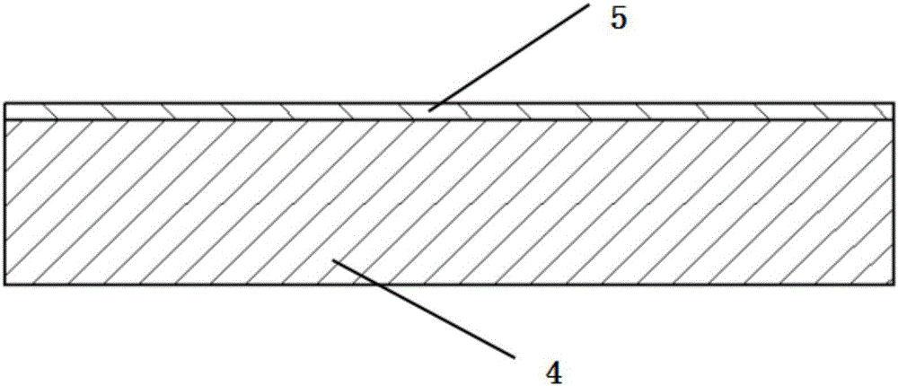
[0050] a) After the silicon wafer 4 is polished and cleaned, as a silicon lining board, one side of the silicon lining board is selected to face up and placed in a dry oxygen oxidation reaction furnace, and pure oxygen is introduced into the reaction furnace, and the temperature is 1000 ° C. , deposit a layer of SiO on the front side of the silicon wafer 4 by thermal oxidation 2 , to obtain a front side with a layer of 1μm thick SiO 2 The silicon liner of layer 5 is denoted as silicon liner A;
[0051] b) SiO on silicon substrate A 2 Coat the surface of layer 5 with a layer of SU-8 photoresist as a mask, and open a window on the photoresist layer, then immerse it in the BOE solution, place it at room temperature until the silicon wafer 4 is exposed by etching at the window, take it out and clean it, and r...
Embodiment 3
[0062] The application of the micro-nano secondary structure mold described in Example 1 in the preparation of micro-nano materials is characterized in that: the application is carried out according to the following method (taking PDMS as an example):
[0063] 1) Soak the mold in the silanization agent of the fluorosilane solution, soak for more than 2 hours at room temperature, perform silanization and hydrophobic treatment on the surface, then wash and dry to obtain the hydrophobic treatment mold, and set it aside;
[0064] 2) Prepare PDMS prepolymer with PDMS base material and PDMS curing agent at a mass ratio of 9:1~10:1. Then add silicone oil and mix thoroughly again to obtain pouring fluid;
[0065] 3) Pouring the configured pouring solution on the surface of the mold with micro-nano grooves after hydrophobization treatment, and gradually degassing after maintaining at 0.02MPa for 20 minutes, and then curing at 70°C for 100 minutes to obtain cured PDMS;
[0066] 4) Care...
PUM
| Property | Measurement | Unit |
|---|---|---|
| length | aaaaa | aaaaa |
| thickness | aaaaa | aaaaa |
| thickness | aaaaa | aaaaa |
Abstract
Description
Claims
Application Information


